Test and measurement forms a pivotal phase validating full functionality across printed circuit board (PCB) assemblies during the product development cycle. Specialized spring contact probes help establish temporary connections between the device under test (DUT) and external testing equipment.
This article provides an overview of PCB test probes focusing on spring contact mechanisms. We analyze probe architectures, key properties, usage scenarios and evolving innovation trends.
Contents:
- Role of Probing in PCB Testing
- Spring Contact Probe Working
- Probe Characteristics
- Probe Architecture Variants
- Applications Case Studies
- Latest Advancements
- Comparison Summary
- Conclusion
Role of Probing in PCB Testing
Probing allows applying test signals or stimuli on a printed circuit board assembly and capturing responses through consistent physical access to various nodes across the product’s copper interconnects, pads, components etc.
Spring probes enable this non-permanent access without soldering test hooks saving time and avoidance of heating boards beyond glass transition temperatures. The spring mechanism also accounts for considerable tolerance in planar, vertical or angular misalignments.
We next look at the basic working principle behind spring contact probes.
Spring Contact Probe Working
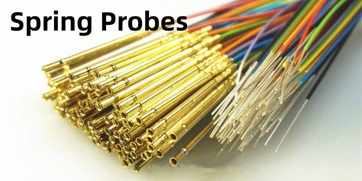
Spring probes utilize an internal spring mechanism, typically made from Beryllium Copper alloy or Stainless Steel. An axial or transverse force gets applied either manually or pneumatically on the plunger pin which compresses the spring thereby extending out the tip to make contact with the board through metal pads or traces.
The spring provides the restoration force retracting the tip when pressure is released post testing. The tip metal determines hardness performance needed for repeated touchdown durability. Nickel alloy tips suit most applications.
Now we analyze essential parameters for test probes.
Probe Characteristics
Contact Force – Gram force defines tip pressure avoiding pad damage while ensuring scrubs through oxides for stable connection.
Overtravel – Distance travelled by probe tip post initial board contact providing compliance buffer.
Pitch Range – Applicable for probe card arrays supporting various pad/ball pitches
Current Rating – Maximum current capacity limit based on trace widths.
Frequency Range – Bandwidth characteristics critical for RF applications.
Adjustment Range – Manual or automated vertical travel range to accommodate board warpage.
Tip Material – Defines hardness, insertion cycles life. Nickel alloys standard currently.
Temperature Rating – Operating temp range either compensated or uncompensated for thermal expansion of metals.
We next contrast popular architectural styles for test probes.
Probe Architecture Variants
Vertical Probes – Straight up-down linear motion. Allow accessing target pad directly underneath probe body.
45 Degree Probes – Angled probe tips useful for reaching peripheral boards in fixtures or confronting space constraints.
90 Degree Probes – Right angle tips essential for confirming short/open circuits checks possible only through sideways trace access without obstructing nearby components.
Custom Configurations – Bespoke probes meeting exact dimensional, motion or force requirements.
We now highlight some industry applications deploying spring probes.
Application Case Studies
Hardware Debugging – Fine pitch probes enable engineers to validate prototype boards through easy access to internal circuits.
Manufacturing Test – Scalable probe cards serve production testers detecting assembly defects through performing continuity checks.
Lab Evaluation – Engineers characterize impedance, signal integrity parameters by judiciously placing probes without affecting intrinsic board performance.
Compliance Testing – Probes inject electrical stress patterns or monitor responses for various immunity/emissions qualification tests.
Latest Advancements
Evolution continues in spring probe technology through:
Materials – New composites combining high conductivity metals and durable polymers enable extended probe life.
Integrated Sensors – Force sensing probes for closed loop force control preventing over-compression.
Interface – Smart probes with digital interfaces relay real-time telemetry for automated test optimization.
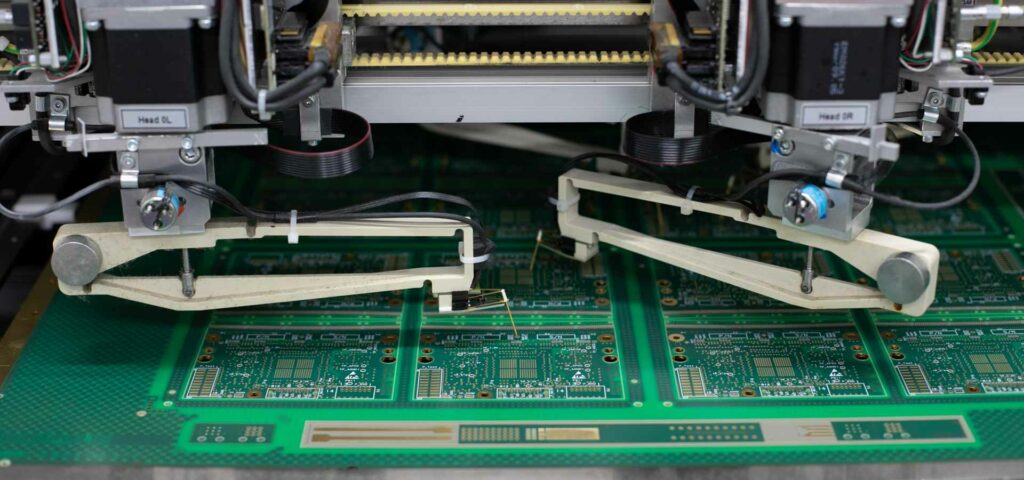
Robot Integration – Automate probe placement through programming robotic arms enabling test parallelization.
Comparison Summary

Finally, the table below contrasts fundamental differences across basic probe types:
| Parameter | Vertical Probe | 45 Degree Probe | 90 Degree Probe |
|---|---|---|---|
| Orientation | Straight Vertical | Oblique | Transverse Horizontal |
| Pad Access | Underneath Probe | Adjacent Pads | Remote End of Trace |
| Space Efficiency | Low | Medium | High |
| Design Complexity | Simple | Moderate | Complex |
| Cost | Low | Medium | High |
Conclusion
In summary, spring contact probes deliver consistent temporary electrical access sought across debugging, characterization and functional validation of PCB hardware assemblies across the product development continuum – from prototype build to sustained manufacturing. Advancement in probe materials and integration of sensing/automation promises to enhance probing efficacy for next-gen testing needs.
I hope this piece provides a useful high-level perspective. Please share feedback or queries through comments!


