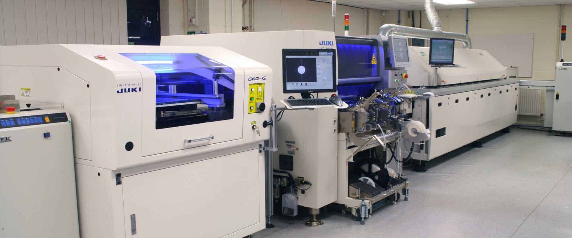
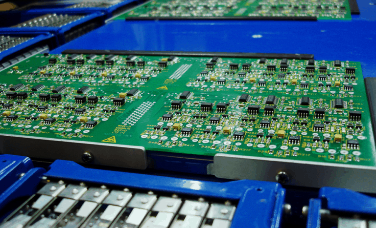
A SMT assembler refers to a manufacturing machine designed to automate the placement and soldering of surface mount technology (SMT) electronic components onto printed circuit boards (PCBs). SMT assemblers, also known as SMT pick-and-place machines, help achieve high throughput assembly of the small devices that enable modern miniaturized electronics.
Understanding SMT assembler capabilities and operation is invaluable for any organization looking to efficiently scale PCB assembly from the lab to mass production environments.
Why Utilize SMT Assemblers for Electronics Manufacturing?
Several compelling reasons are driving adoption of SMT assembly equipment across electronics sectors:
Component Miniaturization
The semiconductor industry’s relentless component size reduction through advanced wafer fabrication and packaging technologies is leading to device packages too small and dense for manual placement.
Rising PCB Complexities
Increasing onboard power delivery, signal speeds, and real estate constraints impose component position accuracy and orientation specifications surpassing human precision.
Production Scale Economies
Transitioning beyond low volume manufacturing necessitates dramatically faster throughput exceeding manual assembly rates. High mix flows also leverage intelligent job setup tooling.
Process Repeatability & Traceability
SMT machines facilitate programming repeatable device placements meeting stringent medical and aerospace certification criteria while logging precise build records.
Technical Overview of SMT Assembly Machines
Modern SMT assembler platforms utilize sophisticated mechanisms to fulfill demanding electronics production:
Feeders
Feeders present device reels or trays to supply components consistently allowing rapid sequencing of differing device types. Tape or stick magazines and vibratory bowls manage small form factors.
Pick Heads
Programmable pick heads with custom nozzles handle device sizes spanning 01005 passives to large QFNs, BGAs, and connectors with indefatigable speed and precision through pneumatic, servo electric, or piezo actuation.
Optical Alignment
Integrated microscopes and imagers facilitate 2D/3D optical recognition aligning PCB targets with device placement locations within fractions of a micron enabling high first pass yield.
Transport Mechanisms
Robust mechanical designs incorporating linear motors, precision rails, and stiffness balancing leverage dynamic analysis optimizing acceleration profiles hitting rates up to 150,000 chip placements per hour minimizing board indexing times through high speed transport.
Thermal Control Stations
Specialized preheaters warm boards to reflow temperatures while chilled vacuum nozzles prevent premature solder melting allowing reliable positioning despite powder coated tacky flux and intricate BGA assemblies requiring perfect alignment.
Standard Features of SMT Assembly Machines
Most SMT assembler platforms offer a breadth of standard functionality:
- Automatic tool change of feeders/nozzles minimizing change overs
- Onboard component libraries streamlining new device support
- Height measurement for coplanarity inspection
- Automatic calibration routines maintaining precision
- Real time production dashboards with analytics/traceability
- Conveyers, buffers, rail transfers flexible factory integration
- Offline programming software reducing setup bottlenecks
- Customizable process step tooling like flux deposition
Prominent Configurations of SMT Assembly Solutions
Diverse options exist scaling from startup needs to tier 1 high volume manufacturing:
| Category | Typical Features | Component Scope | Throughput Speed | Investment Level |
|---|---|---|---|---|
| Entry Level Machines | Compact <1m^2 footprint, basic automation & vision, single head, research/low volume use cases | Passives, SOICs, QFNs, small connectors, CSPs | 500-3500 CPH | $<50K |
| Mid Tier Assembly Systems | Dual head flexibility, component/board flip, advanced process options like paste print, laser fiducials, integrated 3D inspection | 01005s to large BGAs/LGAs, SiPs, stacked components | 5K-13K CPH | $100K-$250K |
| High Speed Modular Lines | Quad head options, multi-rail transport, traceability, high accuracy large board capacity (21”x28”), robotic load/unload automation | 01M pitch ICs, wafer/panel components, large SiPs, laser soldering, high density interconnects | >30K CPH+ | $500K+ investment |
Typical SMT Assembly Machine Hardware Architecture
Modern SMT assembly equipment share a common modular architecture composed from base units:
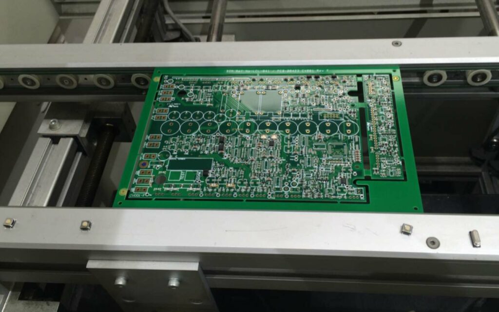
PCB Assembly Flow Through the Assembler
- Input buffer stage stores raw PCB panels and details assembly job programming parameters
- Flux deposition preps PCBs by outlining component placement sites increasing solder adherence
- SMT pick and place heads select devices from feeders mounting them precisely on fluxed pads
- Post placement optical inspection validates position accuracy meets tolerance requirements
- PCB reflow oven heats devices melting solder forming reliable electrical interconnects
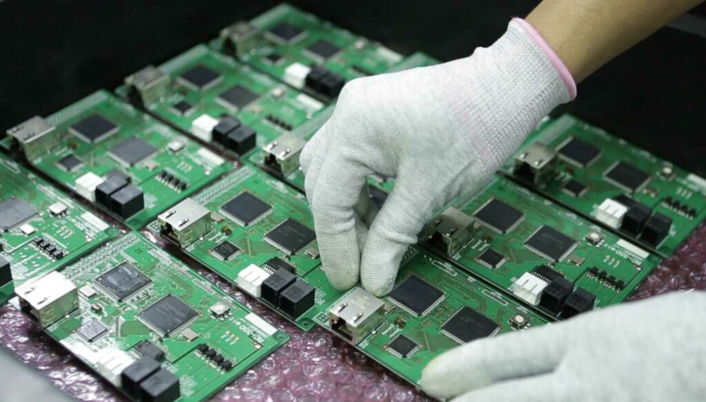
- Output quality check implements tests like in-circuit testing or x-ray judging successful device bonds
- Unload buffer stage manages completed panel inventory ready for further system integration
Optimizing SMT Assembly Machine Performance
Achieving maximum production quality and yield from SMT assembly equipment relies on several best practices:
1. Establishing Trusted Component Libraries
Certifying device package dimensions and test protocols curtails run delays from poor picks. Libraries also assign optimized nozzle types.
2. Validating PCB Design Guidelines
Simulating assembly and reflow via specialized DFM analysis software catches issues preventing errors like tombstoning before reaching the factory floor.
3. Monitoring Feeder Setup
Proactive maintenance programs address worn tape reels while strategic organization groups similar devices minimizing change over delays.
4. Optimizing Reflow Profiles
Custom thermal profiling ensures optimal preheat ramp, soak duration, and cooling control between device melting and PCB damage thresholds unique to each populated board design and solder paste alloy.
5. Qualifying Nozzle Types
New component forms may require custom pick tools optimized balancing strength, precision, and release cues tuned through measurement of characteristics like part height, tackiness, and placement force sensitivity during trial runs.
Conclusion
SMT assemblers are rapidly transforming electronics manufacturing unlocking unprecedented economies of scale through automating precision component integration even as packages hit atomic scale dimensions. Configurable options meet needs across research, low volume, prototyping, and mass production environments while modular architectures maintain upgradability as technologies like advanced optical alignment, thermal management, and autonomous quality control analytics mature. Organizations leveraging SMT assemble capabilities position themselves advantageously leading disruptive connected device revolution underway through access to cutting edge techniques circumventing limitations constraining competitors only able to rely on legacy human-centric placements.
Frequently Asked Questions
How is the optimal component placement sequence determined for complex, high density PCB designs?
Intelligent pathfinding algorithmsparse pairing device size/masses with corresponding nozzle types alongside board thermal reliefs minimizes cumulative offset torques preventing skipped placements from collisions while meeting symmetry objectives.
What breakthrough innovations are emerging from integration of artificial intelligence into SMT assembly machines?
Closed loop optimization tapping 24/7 operational data instantiated through neuron simulation techniques autonomously customizes pick sequences maximizing yield revealed through probabilistic inspection analytics while minimizing changeover downtimes forecasting feeder replenishments.
How are ultra-fine pitch wafer scale components integrated practically leveraging SMT assembly?
Advances in flux viscosity reduction and spray deposition accuracy facilitate reliable temporary tacking anchoring fragile sub 100 micron pitch silicon interconnects until laminated substrate bonding reinforces durable mechanical integration.
Why has augmentation/virtual reality (AR/VR) seen adoption assisting SMT assembly technicians?
AR overlays real-time component alignments against reference footprints aiding tweak adjustments meeting tolerance requirements while VR simulations build placement proficiency sans equipment access downtime. Both accelerate competency.
Where do solder fabricated interconnect alloys stand today regarding lead free requirements and operating temperature ranges?
High silver blends rival traditional tin-lead solder reliability metrics now at 260°C reflow peaks easing high density integration marching towards IoT edge node endpoints stretching environmental resilience thresholds.


