Introduction
Getting a quote for a custom printed circuit board (PCB) can be a daunting task, especially if you’ve never had PCBs manufactured before. There are many factors that go into determining the final cost, from the board’s size and layer count to the quantity being produced. Understanding these key considerations will help you get the best possible price when sourcing prototype and production PCBs.
In this comprehensive guide, we’ll walk through the entire PCB quoting process, from generating fabrication and assembly quotes to negotiating with manufacturers. We’ll also provide tips on optimizing your PCB design to minimize costs. Follow these steps to get a competitive quote that fits your budget and requirements.
Overview of the PCB Manufacturing Process
To understand what goes into generating a PCB price quote, it helps to first understand the basic manufacturing process:
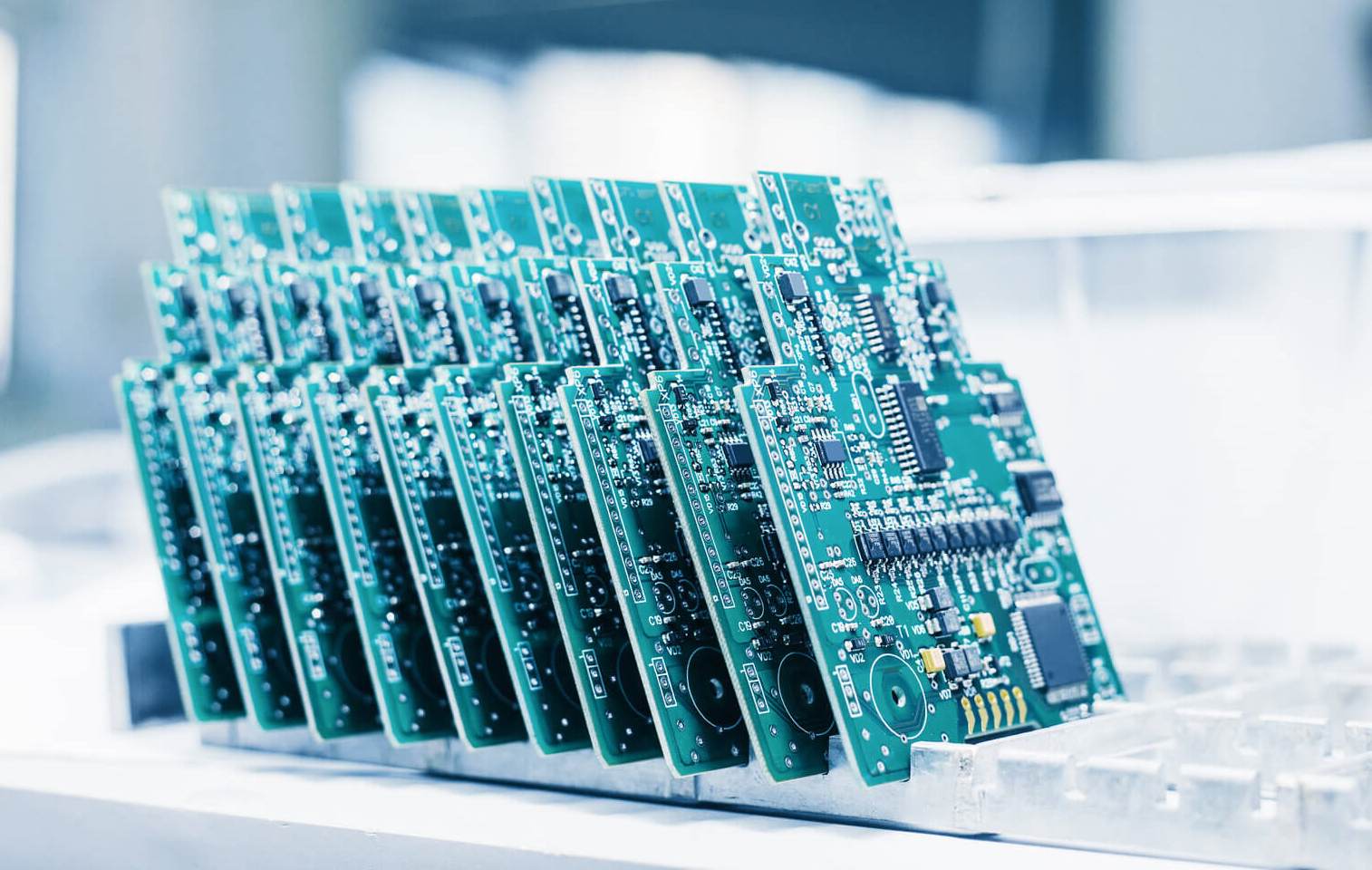
PCB Fabrication
This involves creating the raw printed circuit board from your Gerber files. The key fabrication steps are:
- Imaging – A photosensitive layer is added to the copper clad laminate. The Gerber files are used to image the PCB pattern onto this layer.
- Developing – The unexposed photosensitive layer is washed away, leaving only the desired copper traces.
- Etching – The exposed copper is etched away, isolating the traces.
- Stripping – The remaining photosensitive layer is removed.
- Testing – The finished boards are electrically tested.
PCB Assembly
This is where components are soldered onto the fabricated PCB. Main assembly steps are:
- Printing – Solder paste is printed or dispensed onto pads.
- Pick and place – Components are precisely placed onto the PCB.
- Reflow – The boards pass through an oven, melting the solder to form solder joints.
- Testing – Assembled boards are tested for proper function.
Factors like minimum trace widths, thin materials, and fine pitch components will increase assembly costs.
Key Factors That Influence PCB Cost

There are a number of key factors that PCB manufacturers consider when generating their pricing:
Board Size
In general, larger boards will cost more to produce. This is because larger boards:
- Take up more space on the manufacturing panels. Less boards fit per panel.
- Require more materials (substrate, copper, etc.).
- Are more difficult to handle and process.
To save costs, avoid oversizing your PCB and reduce board dimensions when possible.
Layer Count
Boards with more copper layers are more expensive to fabricate. Reasons for increased costs:
- Additional lamination and imaging steps are required.
- More materials are consumed, particularly copper foil.
- Reducing trace widths and spacing gets more difficult.
- More advanced processes may be needed for fine features.
Carefully evaluate whether all layers are necessary. Can routing be optimized to use fewer layers?
Minimum Trace/Space
The finest trace width and spacing that can be achieved will impact costs.
Tighter tolerances require:
- More accurate imaging and etching equipment.
- Thinner copper weights, which drives up material costs.
- Potentially special substrates if very thin dielectrics are needed.
- More fragile boards that have lower yields.
If possible, keep minimum features above 5/5 mil (0.127mm) trace/space.
Materials
- Substrate – FR-4 glass epoxy is the least expensive. Get quotes on high-frequency (eg Rogers) substrates versus standard FR-4.
- Copper Weight – Heavier copper is more costly. See if 1oz copper will work instead of 2oz.
- Immersion Gold – Upcharge for ENIG surface finish over standard HASL.
- Solder Mask Color – Standard green is cheapest. Other colors add cost.
Hole Sizes/Tolerances
- Small drill bits are prone to breakage, driving down yields.
- Tight hole tolerances require precise drilling equipment.
- Plated slots and cutouts require additional processing steps.
Open up tolerances as much as your design allows. Avoid holes under 0.4mm if possible.
Panel Utilization
Manufacturers optimize panel space by arranging multiple PCB designs onto larger panels. Densely packing boards leads to material savings.
For prototype runs, you’ll be quoted based on single board pricing. But for production, be sure to optimize panel utilization yourself during layout.
Testing/Inspection
Testing and inspection (flying probe, AOI, x-ray) all add cost. Decide what testing is needed versus what’s optional.
Lead Time
Standard lead times are ~5 days for prototypes, ~10-15 days for production. Rush services have significant upcharges.
Build in sufficient time when planning your project schedule.
Quantity
Upfront costs like fabrication tools are amortized over more boards. This leads to reduced per board pricing at higher quantities.
See what breaks make sense for your project’s budget (e.g. 10, 25, 100).
Design for Manufacturability
DFM practices like those outlined in this guide will help reduce quoting variables that add ambiguity or drive up costs when going to manufacturing.
Getting PCB Quotes: Generate, Compare, Negotiate
Now that we’ve covered the key factors that affect PCB pricing, let’s walk through the process of actually obtaining quotes.
1. Generate Quotes
Start the process by requesting quotes from several manufacturers. Most offer instant online quoting forms on their website. Be prepared to provide:
- Gerber files – Ensure they are fully up to date first!
- BOM/component datasheets – For assembly quotes
- Preferred construction – Layers, material, finishes, etc.
- Quantities – Protos, pre-production, mass production
- Lead times – Standard or expedited
- Special requirements – DFA/LF fabrication, testing, etc.
To cast a wide net, get quotes from:
- Domestic manufacturers
- Overseas/China-based manufacturers
- Large vs small manufacturers
- Generic vs specialized manufacturers
2. Compare Quotes
Once quotes start coming in, enter them into a spreadsheet for easy comparison. Some key factors to track:
- Base pricing – Fabrication, assembly, stencil
- Cost impact of each material/feature
- Lead times
- NRE/tooling costs
- Potential volume discounts
- Total cost per board at various quantities
- Feasibility of features/tolerances
Compare line item costs and look for inconsistencies. Are some manufacturers vastly overcharging for certain operations?
3. Negotiate for the Best Price
With quotes from multiple sources in hand, you are now in a strong position to negotiate!
Some key strategies:
- Focus negotiations with 1-2 manufacturers you want to work with. Get to know their capabilities.
- Make them compete! Have them re-quote if certain manufacturers give you better pricing on specific items.
- Keep quantity vague. Ask them to re-quote 10, 25 or 100 boards and see how it changes.
- Bundle fabrication + assembly for higher leverage.
- Offer them more business for lower costs, but don’t overcommit.
- For core processes, push back on costs that seem far outside industry norms. Don’t overpay for basic operations.
- If quoted lead times don’t work, ask if expediting/rush is possible. Get fees.
- Be willing to compromise on lower-priority requirements to reduce costs.
Top Tips for Optimizing Your Design to Reduce Costs
Beyond getting good quotes, you can take proactive measures to design your PCB with manufacturing costs in mind. Follow these design-for-manufacturability (DFM) guidelines:
Board Size
- Make your PCB as small as possible while still fitting components.
- Standard sizes like 100mm x 100mm are economical.
- For prototypes, err on the smaller side. Scale up later for production.
Layers
- Minimize layer count. Can routing be tightened up to use fewer layers?
- If RF, carefully evaluate if microstrip transmission lines need a ground plane.
- Don’t use planes as fills—use hatched polygons.
Traces and Spaces
- Design with 5 mil/5 mil trace/space minimums.
- For digital signals, can 10 mil/10 mil work? Widening saves substantially on cost.
- Minimize the use of 3mil/3mil traces unless required by high-speed layout.
Vias
- Avoid via-in-pad—use thermal relief pads instead.
- Minimize or eliminate buried/blind vias. They require more complex plating.
- Don’t tent unused through-hole vias. Leave them open.
Hole Sizes
- Keep hole sizes above 0.4mm minimum.
- Open up tolerances on hole sizes as much as possible.
- Avoid slotted holes. Use multiple drilled holes instead if possible.
Copper Weights
- For outer layers, use 1oz copper instead of 2oz if your design allows it.
- Evaluate if thinner copper weights are feasible for inner layers.
Masks and Finishes
- Use standard green solder mask unless other colors are absolutely needed.
- Avoid expensive ENIG finish if HASL will work.
Components
- Choose package footprints wisely. QFNs and BGAs are harder to assemble and inspect.
- Avoid components with tight pitch leads unless essential.
- Use design landmarks for automated inspection.
Frequently Asked Questions
What are the main costs involved in PCB manufacturing?
The primary costs involved in PCB manufacturing are materials, labor, equipment time, and overhead. Materials such as substrate, copper foil, soldermask, and surface finishes account for a significant portion of fabrication costs. Labor is required for activities like imaging, stuffing boards, inspection, and testing. Specialized equipment like photoplotters, etching machines, and drilling/routing tools is expensive, so maximizing their utilization saves money. Overhead costs like facilities and equipment maintenance/upkeep must be covered in the pricing as well.
Should I get quotes from domestic or overseas manufacturers?
It’s a good idea to get quotes from both domestic and overseas manufacturers. Domestic PCB shops can provide quicker turnaround times and better communication/support due to proximity and shared timezones. However, their pricing is often higher. Overseas manufacturers, particularly in China, can produce PCBs at extremely competitive costs but usually have longer lead times. Include both in your initialquoting process, then decide based on your budget, schedule requirements, and where you feel most comfortable sourcing from.
How many PCB quotes should I get?
As a rule of thumb, plan to get quotes from at least 3-5 different manufacturers. This allows you to sample a decent cross-section of pricing and capabilities. Any less than 3, and you won’t have enough data points to effectively compare and negotiate. Be careful going much above 5 however, as getting quotes can be a time consuming process. Focus your efforts on a few manufacturers that seem well aligned to your project’s needs.
Should I inform manufacturers that I am getting multiple quotes?
Absolutely, you should let all the manufacturers know that you are collecting quotes from several different sources. This is perfectly acceptable practice in the industry. Oftentimes, revealing that you are benchmarking pricing will motivate manufacturers to sharpen their quoted pricing to win your business. Just avoid explicitly telling one manufacturer the exact quote you received from another.
What are NRE and tooling charges? Should I expect to pay these?
NRE (Non-Recurring Engineering) and tooling charges cover the upfront costs that a manufacturer incurs when setting up for a new custom PCB design. This includes fabricating phototools/printing screens, performing DFM checks, generating CAM data, procuring special materials, and building custom test fixtures. For prototype quantities, NRE is sometimes waived or minimal. But for production runs, you should expect to pay NRE fees, especially for complex boards. Treat these as investments that allow achieving lower unit pricing.


