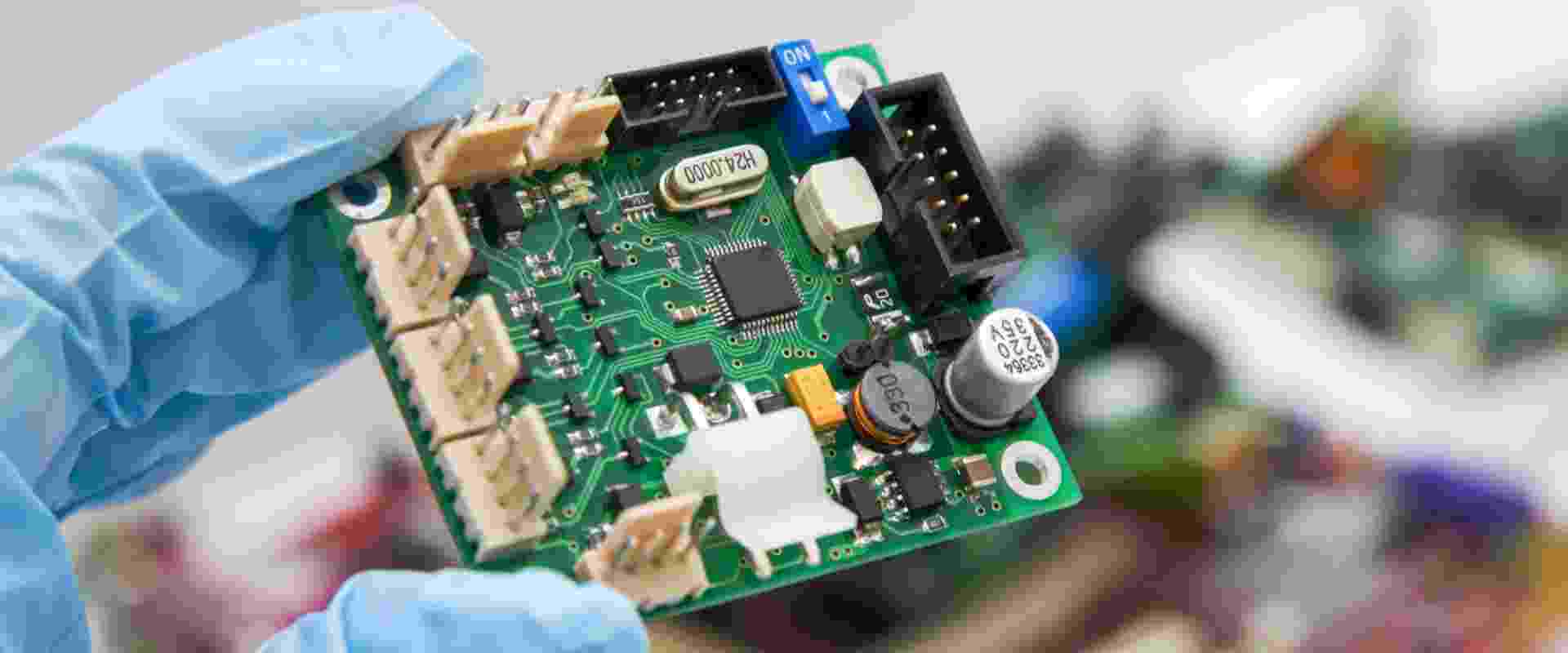
Printed circuit boards (PCBs) provide the fundamental interconnect platform upon which nearly all modern electronic devices and systems are constructed. PCBs are utilized universally due to their ability to economically and reliably support the functionality, density, and assembly requirements of sophisticated electronics.
Understanding why PCBs play such an indispensable role across every category of electronics requires examining key attributes that have made them the preferred foundation for electronic circuitry.
Structured Physical Platform
PCBs establish the physical structure for securely mounting electronic components and integrating their connectivity. This provides:
- Component support – Provides solid foundation to mechanically affix components
- Layered construction – Enables compact multilayer circuit architectures
- Durable packaging – Robust epoxy laminate materials protect components
- Defined dimensions – Standardized PCB sizes and thicknesses for manufacturability
- Modular sections – Different assembly areas can be compartmentalized on boards
The PCB substrate delivers a robust yet adaptable physical platform suited for electronics.
Electrical Interconnectivity

The conductive copper traces etched on PCBs establish pathways for electrons to travel between attached components. This enables:
- Power distribution – Transfer power from sources to components needing electricity
- Grounding – Provide common ground reference points for voltage regulation
- Signal routing – Propagate electric signals between components for data and control
- Component terminals – Copper pads connect to component leads or solder balls
- External interfaces – Board-edge connectors link PCB assemblies to cables and wiring
PCBs integrate and bridge all electronic elements through purposeful electrical interconnects.
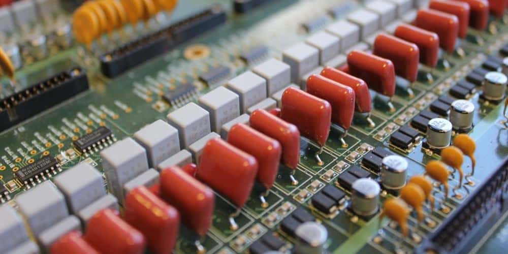
Miniaturization
PCB fabrication technologies facilitate extremely compact circuit architectures not feasible with individual wires or cables, including:
- Fine line traces – Narrow trace widths conserve space on dense boards
- Tiny vias – Small drilled holes allow vertical jumping between layers
- Microwave materials – High-frequency dielectrics enable thinner circuit layers
- Embedded passives – Passive components like resistors can be built into layers
- High density interconnects (HDI) – Extremely compact external and internal component spacing
Advanced PCBs permit far greater miniaturization than alternatives allow.
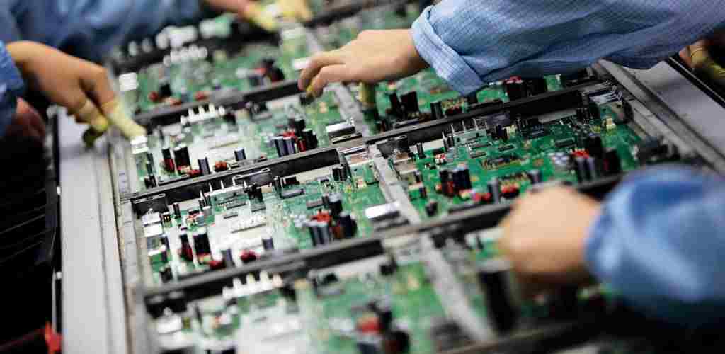
Efficient Processes
PCB manufacturing leverages highly automated volume production, enabling:
- Economies of scale – Unit costs decrease as volumes increase
- Production gear – High throughput equipment for fabrication, assembly, test
- Repeatable precision – Process uniformity and accuracy benefits reliability
- Quality controls – Statistical control procedures ensure consistency
- Lean workflows – Waste reducing production workflows maximize efficiency
Process sophistication yields affordable, high quality PCBs at scale.
Simplified Assembly
PCB construction and materials simplify automated production assembly, including:
- Solder pads – Plated thru-hole and surface mount pads enable reliable soldering
- Component legends – Silkscreen markings identify part locations and orientations
- Assembly equipment – Pick-and-place machines easily mount components on boards
- Solderability – Hot air, wave, or reflow attachment processes
- Efficient workflows – Streamlined processes avoid errors and delays
PCBs are purpose-built to optimize electronics manufacturing throughput and productivity.
Configuration Flexibility
PCBs can be adapted to suit diverse applications and evolving needs:
- Design iterations – Circuit schematics and board layouts can be changed
- Multi-layer – Stacked layer construction creates complex architectures
- Component libraries – Vast arrays of standardized electronic parts are available
- Materials selection – Substrate properties align with application needs
- Additive manufacturing – 3D printing permits on-demand customization
PCBs provide extensive options to tailor electronics form and function.
Advanced Packaging
Critical components require compact, high performance PCB packaging:
- Chip packaging – Chips mount directly to boards in BGA, QFN, etc packages
- Known good boards – 100% electrical testing verifies PCB integrity
- EMI shielding – Protects sensitive mixed-signal and RF devices
- Thermal dissipation – Spreads and sinks heat from high power components
- Environmental protection – Conformal coatings safeguard against contaminants
PCBs enable advanced semiconductor and electronics packaging architectures.
Reliable Functionality
Rigorous design, testing, and controls provide dependable PCB performance:
- DFx methodologies – Design for manufacturability, testability, etc.
- Modeling and simulation – Verifies circuit integrity before manufacturing
- Inspections and testing – At multiple stages from bare boards through full assembly
- Lifecycle analysis – Stress testing and simulation assess operational durability
- Process controls – Statistical process monitoring tracks variances
Disciplined PCB engineering delivers reliable, consistent platform functionality.
PCB Innovation
Ongoing PCB advancements expand electronics possibilities:
- Materials research – High-speed, high-frequency, and high-temperature materials
- Flexible circuits – Dynamically flexing interconnections
- Embedded actives and passives – Discretes built into the PCB layers
- Additive processes – Printed electronics and 3D structuring
- Heterogeneous integration – Mixing components like ICs within board
Continuous PCB innovation fuels new generations of electronics.
In summary, PCBs enable electronics through their unmatched ability to economically interconnect components while meeting density, performance, manufacturability, and reliability demands. As electronic systems grow more sophisticated, PCBs will continue evolving as the foundational platform upon which these innovations are built.
FQA
How have PCBs contributed to the increasing miniaturization of electronics?
PCBs facilitate miniaturization through small geometry fabrication techniques like high density routing, microvias, embedded passives, advanced chip packaging, and fine line flexible circuits.
What are some differences between consumer and industrial PCBs?
Consumer PCBs focus on low cost manufacturing while industrial PCBs require extended temperature ranges, power handling, vibration resistance, and longer lifecycles.
How do the materials used in PCBs impact their functionality?
Materials determine PCB electrical and thermal characteristics. Factors include dielectric constant, dissipation factor, CTE, Tg, thermal conductivity, and frequency response.
What role does modeling and simulation play in the PCB development process?
Modeling and simulation predicts electrical, thermal, vibration, shock, and fabrication behaviors to improve design performance and manufacturability before building prototypes.
How has fabrication technology evolved to enable greater PCB capabilities?
Evolutions in lithography, laser drilling, robotics, additive processes, inspection systems, automation software, and data analytics have enhanced PCB manufacturing sophistication.


