Introduction
Electronics manufacturing is the process of designing, fabricating, assembling and testing electronic devices and systems. The manufacturing sequence transforms raw materials like silicon wafers, components and circuit boards into finished electronic products.
This guide provides an overview of the major stages and key steps involved in manufacturing electronics. We will examine the workflows for printed circuit board (PCB) fabrication, component manufacturing, PCB assembly, product testing and enclosure fabrication that enable the mass production of electronic devices.
Understanding the end-to-end electronics production process allows companies to optimize manufacturing operations, ensure quality and bring innovative products to market faster.
Printed Circuit Board Fabrication
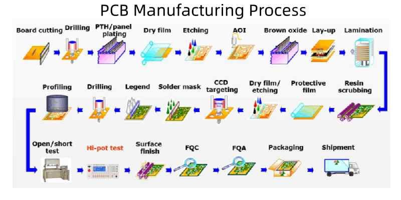
Printed circuit boards (PCBs) form the foundation of electronics manufacturing. PCBs provide the mechanical structure to mount and interconnect electronic components. The steps to fabricate a PCB are:
PCB Design
Engineers create board layouts and generate Gerber data and drill files using EDA software tools like Altium, Cadence Allegro and OrCAD.
Materials Selection
The PCB manufacturer chooses compatible materials including the substrate, copper weights, finishes, stiffeners etc. based on design requirements.
Imaging
Photolithography transfers the PCB layout onto each layer by selective exposure and development of photoresist.
Etching
Unwanted copper is etched away to form the pads, traces and features. Wet chemical etching or plasma dry etching are commonly used.
Lamination
Sheets of dielectric prepreg and copper foil are stacked up and fused together under heat and pressure.
Drilling
Holes are mechanically drilled or laser drilled to create vias andcomponent holes.
Plating
Metals like copper, tin, nickel and gold are plated onto pads and holes for conductivity and solderability.
Soldermask & Silkscreen
The soldermask insulator and component legend silkscreen are applied.
Testing
In-circuit, flying probe and optical inspection testing validates PCB function.
Panelization
PCB panels are broken into individual boards by routing, punching or scoring.
The fabricated PCBs are now ready for population with components.
Component Manufacturing
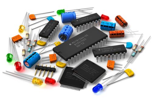
Electronic components that mount onto the PCBs are fabricated using specialized processes.
Semiconductor Fabrication
Chips like microprocessors and memory are manufactured on silicon wafers using lithography, doping, layering, etching and other frontend processes. The back-end sequence dices, packages and tests the chips.
Passive Components
Resistors, capacitors, inductors and transformers are fabricated on assembly lines. Materials like ceramics, epoxy, wires and leads are combined to build each component type.
Electromechanical Parts
Connectors, switches, relays and other electro-mechanical parts are fabricated by combining insulation materials, metal contacts, springs, wire leads and plastic or metal housings.
PCB Assembly Components
Sockets, spacers, standoffs, heatsinks and mounting hardware are molding or machined to specification.
Components from various suppliers come together at electronics assembly factories.
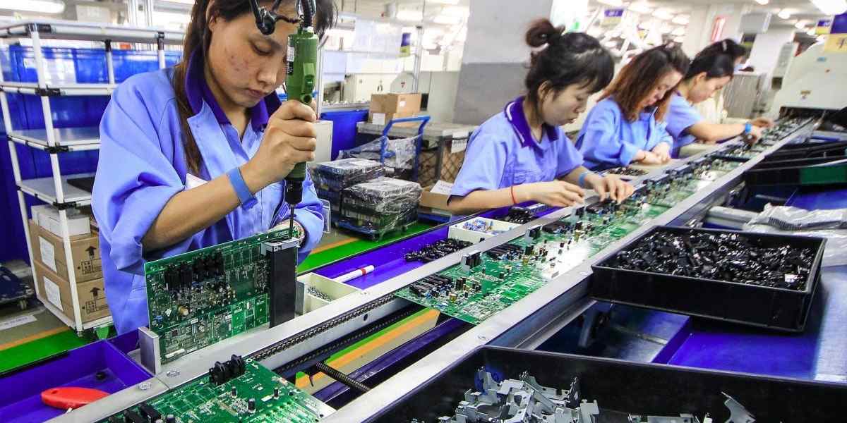
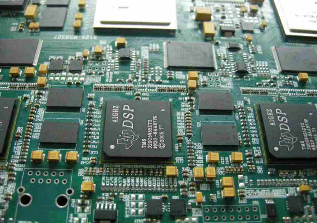
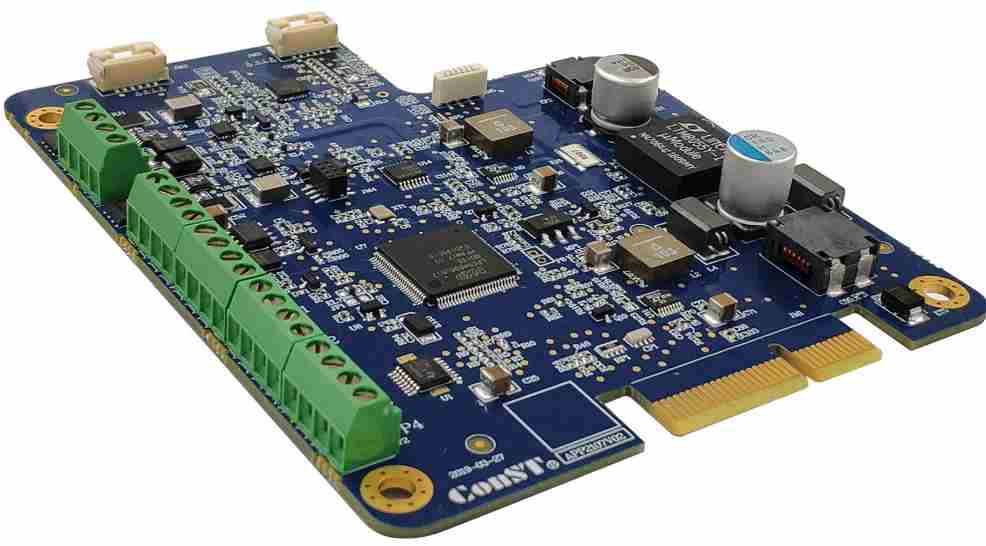
Printed Circuit Board Assembly
PCB assembly, also called PCBA, attaches and solders components onto fabricated PCBs.
Solder Paste Printing
Solder paste is printed or dispensed onto pads where components will be placed. Reflowable solder paste alloys like Sn96.5/Ag3/Cu0.5 are commonly used.
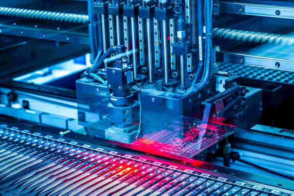
Pick and Place
Robotic pick and place machines accurately populate components onto the PCB from reels, trays or sticks. Vision and fiducial recognition ensure precision.
Reflow Soldering
The populated board passes through a reflow oven to heat and fuse the solder paste, forming reliable mechanical and electrical joints.
Conformal Coating
A protective polymer coating may be selectively applied to the assembled PCB to prevent corrosion and environmental damage.
Post Solder Processes
Additional soldering operations may be done like hand soldering or wave soldering to attach larger components and connectors.
Cleaning
Flux residue removal improves aesthetics and prevents ionic contamination that could impact functionality.
The fully assembled PCB with all components attached is known as a printed circuit board assembly (PCBA) and is now ready for enclosure integration and system-level testing.
Product Testing and Validation
Testing at various stages of production ensures that the final product meets specifications.
In-Circuit Testing
An electronic “bed of nails” fixture tests PCBs before population to validate connectivity and function using boundary scan and other techniques.
Flying Probe Testing
Programmable flying probes provide electrical testing for boards that do not have fixtures designed.
Automated Optical Inspection
2D and 3D optical inspection compares assembled boards against a known good example to identify defects.
Functional Testing
Once enclosed, finished products undergo power-on functional testing to validate performance across operating conditions.
Environmental Stress Screening
Temperature, vibration and voltage stress screening accelerates latent defects to improve reliability.
Compliance Testing
Products are tested for conformance with safety, EMI/EMC, performance and regulatory standards like UL, CE or FCC.
Thorough testing at multiple stages ensures defects are identified early and products meet specifications consistently.
Enclosure Fabrication and Integration
Electronic products require enclosures for protection, aesthetics and usability. Common methods for enclosure fabrication include:
Injection Molding
Polycarbonate, ABS and other thermoplastics are injection molded into complex, high precision enclosures and housings.
Sheet Metal Fabrication
Steel, aluminum and other metal sheets are cut, formed and welded into enclosures using presses, CNC machines and other metal working equipment.
Casting
Molten metal is poured into a mold cavity and allowed to solidify to produce cast metal parts like bases and shields.
Additive Manufacturing
3D printing builds up enclosures additively from resins, powders or filaments for fast prototyping and custom designs.
The electronics sub-assemblies are integrated into the enclosure and interconnected. Additional processes like branding, coatings and surface finishes are done before final functional testing and shipment.
Summary of the Electronics Manufacturing Sequence
To quickly recap, the key production stages to build electronic devices are:
- PCB Fabrication – Make bare printed circuit boards
- Component Manufacturing – Fabricate resistors, ICs, connectors etc.
- PCB Assembly – Solder components onto boards
- Testing – Validate operations at component and system levels
- Enclosure Fabrication – Make housings and chassis
- System Integration – Interconnect sub-assemblies into complete product
- Functional Testing – Power-on test of finished product
- Packaging and Shipment – Final checks before sending to customer
Understanding the full electronics manufacturing process helps engineers optimize designs for efficient production. It also assists manufacturing personnel and managers in identifying issues and continuously improving processes to deliver high quality electronics products on schedule.
Frequently Asked Questions
What are some key PCB design considerations for ease of manufacture?
Important considerations include component spacing, thermal management, layer counts, material selection, accessibility of test points and easing assembly by standardizing components. Close collaboration between design and manufacturing teams is advised.
How does automated optical inspection compare with in-circuit testing?
AOI visually checks assembled boards but may miss electrical shorts or opens. In-circuit testing probes actual circuits but requires physical test fixtures. The two techniques complement each other for complete testing.
What joining methods are used in electronics assembly besides soldering?
Other attachment methods include adhesives, press-fit connectors, compression brackets, fasteners and clips. Hybrid joining maybe needed for large modules or to accommodate different Coefficients of Thermal Expansion between parts.
What are some ways to decrease changeover times between product variants?
Some approaches include quick changeover fixtures, using the SMED system to convert setups, modular product designs and flexible automated systems that can easily switch programs or fixtures.
How is reliability ensured during electronics manufacturing?
Reliability assurance practices like HALT stress testing, effective quality control, statistical process control tracking, continuous improvement programs and rigorous testing throughout production combined with sound designs are key to preventing field failures.
This overview summarizes the end-to-end electronics manufacturing process steps companies use to transform designs into functioning products efficiently, affordably and reliably. Let me know if you need any clarification or have additional questions!


