In high speed PCB design, signal propagation delay defines the time taken for electronic wavefronts to traverse interconnects from drivers to receivers. With data rates exceeding multi-gigabits per second, delay directly impacts timing budgets. Understanding key contributors that make up propagation delay enables engineers to model, analyze and optimize high frequency layouts effectively.
This article details various intrinsic and extrinsic factors affecting propagation delay through:
- Origins of delay in transmission lines
- Deriving and calculating delay values
- Modeling delay phenomenon
- Impact on signal integrity
- Mitigation methods – routing, terminations, materials
- Real world estimation and measurement
- Effects on timing analysis
- Applicable examples in systems
Equipped with a wholesome understanding of signal delay intricacies in modern PCBs, engineers confidently design for precision timing closure.
Origins of Signal Propagation Delay
In ideal wires that instantaneously conduct electricity, signals move at almost light speed. But in real-world PCB traces functioning as transmission lines, velocity slows down due to physical effects that constitute delay.
Prime Delay Contributions:
- Resistive Loss
- Capacitive Loading
- Inductive Reactance
- Frequency Dependency
Let’s examine each contributor.
1. Resistive Losses
Copper traces have small but finite resistance that converts some signal energy to heat according to Ohm’s law – restricting charge flow velocity. Higher resistivity copper alloys demonstrate larger delays.
2. Capacitive Loading
Adjacent power/ground planes form parasitic capacitance that charge/discharge, storing energy – slowing signal edges as modeled below:
3. Inductive Reactance
Associated loop inductance interacts with capacitance to create LC tank circuit resonance – with velocity peaking at resonance frequency while lagging on either side.
4. Frequency Effects
As signal spectral content increases beyond ~1 GHz, transmission line effects emerge retarding propagation with additional elements like skin effect resistance and dielectric losses.
With key delay constituents identified, let’s mathematically derive the delay number next.
Deriving Signal Propagation Delay
Propagation delay quantifies the latency incurred as signals traverse transmission line interconnects at finite time compared to ideal instantaneous conduction.
Mathematically, it gets calculated as:
Delay Time (t) = Dielectric Constant (Dk) x Length (L) / Velocity (Vp)
Where,
- Velocity Vp = c / √Dk
- c = Speed of light = 0.2997 mm/ps
For standard FR4 material,
- Dk = 4.5
- Vp = c / √4.5 = 0.14 cm/ps
This forms the basis for first order propagation delay estimates on common PCB dielectric substrates. Building upon the basics, we cover detailed modeling techniques next.
Modeling Propagation Delay
While a constant nominal dielectric velocity works for back-of-the-envelope delay calculations, real-world effects necessitate more sophisticated modeling for high accuracy:
- Frequency dependent material properties
- Skin effect losses
- Quadratic delay across broad spectra
- Routing topology configurations
- Reflections and terminations
Leveraging full-wave 3D field solvers, the propagation delay profile gets simulated across the spectrum capturing frequency and spatial responses for matched empirical results.
Here is a sample plot showing delay varying over 100 MHz to 40 GHz band:
So wideband propagation delay modeling sets expectations for high bandwidth channels early in design phase. Correlation to measured results then validates signal quality.
Next, we examine the effects of uncontrolled propagation delays.
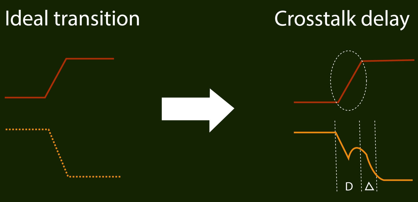
Effects of Propagation Delay on Signals
Unaccounted variable signal propagation delays directly affect:
Pulse Distortion
- Leads to inter-symbol interference errors in data buses
Phase Misalignments
- Causes jitter and synchronization issues
Resonance Peaks
- Ringing accentuates overshoot and ringing
So while designing high speed serial links and parallel buses:
- Match delays of related signals
- Equalize trace lengths in bytes/groups
- Model loaded delay effects
- Verify timing margins post layout
Controlling these parameters maintain signal integrity and stability.
Mitigating Propagation Delay
To alleviate harmful delay effects, a range of design-stage and post-layout mitigations help:
1. Topology Symmetry
Balanced distribution networks maintain relative phase relationships.
2. Matched Delay Routing
Length tuning critical net pairs for simultaneous switching
3. Terminations
Source/load end termination eliminates reflections
4. Material Selection
Choosing substrates as per bandwidth needs
5. Delay Equalization
Retimers recorrect duty cycle and jitter post-layout
So applying suitable delay management approaches from architectural planning to component integration tames effects.
Real World Delay Estimation
While physics-based modeling offers accuracy, simple heuristics also provide practical signal delay estimates:
FR4 Dielectric
- 5 ns delay per foot of trace (@ ~2x speed of light)
- 166 ps per inch of route length
Differential Microstrip impedance Routing
- Delay ~ 140-160 ps per inch depending on layer Dk
So quick heuristics complement detailed analysis particularly when designing channels from related existing systems. Correlation to measurements then validates estimations.
Having covered concepts in depth, we now discuss implications.
Effects on Timing Budgeting and Analysis
With propagation delays directly consuming signal transition margins, proper modeling and budgeting ensures timing closure:
Simplified Timing Diagram
- Source synchronous links need accurate flight times for clock phase alignment
- Setup/hold time margins subtract jitter and delay effects
- Logic paths balance gate and interconnect delay allocations
So comprehensive timing analysis should account for modeled wire delays after placement rather than just assume ideal transmission. This prevents over-constraints skewing optimization.
Finally, we summarize key takeaways.
Summary of Signal Propagation Delay in PCBs
1) Multiple factors like resistive losses, capacitive loading and inductive resonance define intrinsic propagation delay in transmission line PCB traces
2) Careful modeling captures frequency-dependent delay behavior enabling preemptive mitigation
3) Matched delay routing, symmetry and terminations alleviate effects
4) Estimating per inch delay guides analysis without extensive simulation
5) Timing budgets pre-allocate wiring delay alongside logic for positive slack
Getting familiar with the composition and quantified metrics of propagation delay aids PCB designers plan, analyze and mitigate high frequency timing effects right the first time avoiding costly respins.
With this wholesome perspective, engineers discern key considerations when designing interconnect intensive systems to meet signal integrity and performance needs.


