A printed circuit board (PCB) is a board made of insulating material like FR-4 on which components like integrated circuits and resistors can be mounted and interconnected using copper tracks. The number of layers in a PCB refers to the number of copper layers that make up the board.
4 layer PCBs, as the name suggests, have 4 copper layers which are used to route signals and provide power and ground planes. They provide more routing channels than 2 layer boards leading to increased component density and complex routing capabilities. At the same time, they avoid the cost and complexity of boards with 6 or more layers. This makes 4 layer boards a versatile and popular choice for many electronic products.
Benefits of 4 Layer PCBs
Here are some of the key benefits of using a 4 layer PCB:
- Increased routing capability: The two extra inner layers double the routing channels compared to a 2 layer board. This enables routing of more signals in complex designs.
- Good signal integrity: The additional copper provides better power distribution and decoupling. This improves signal quality and integrity.
- Smaller board size: Higher routing density allows components to be placed closer. This reduces the overall board dimensions.
- Flexibility: 4 layers provide a good trade-off between capability and cost. They can be an ideal choice for products that have grown beyond 2 layers but do not yet need 6+ layers.
- Cost: 4 layer boards have become very cost effective to manufacture. They provide significant improvements over 2 layer boards at a small cost premium.
Limitations of 4 Layer PCBs
Some limitations of 4 layer PCBs compared to higher layer count boards:
- Lower routing capacity than 6+ layer boards for highly complex designs.
- Power plane splits can be more challenging than on 6 layer boards.
- Group delay skew issues may occur due to lack of closely coupled signal layers.
- Lower layer count provides less isolation for sensitive analog circuits.
However, with good design practices, these limitations can usually be addressed or mitigated in 4 layer boards.
Typical 4 Layer Stackup Configurations

There are two common stackup configurations used for 4 layer PCBs:
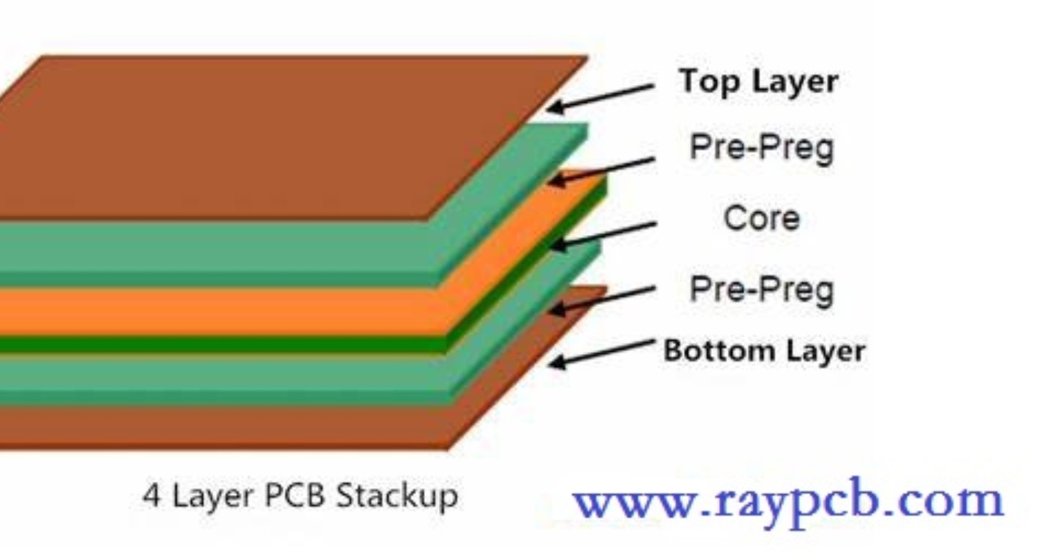
1. Signal-Power-Ground-Signal
This is the most typical and default stackup. The four layers are arranged as:
Layer 1: Signal
Layer 2: Power (VCC)
Layer 3: Ground (GND)
Layer 4: Signal
The signal layers on the outside provide maximum routing space. The VCC and GND planes provide power distribution and shielding in the middle.
2. Signal-Signal-Power-Ground
In this arrangement, the stackup is:
Layer 1: Signal
Layer 2: Signal
Layer 3: Power (VCC) Layer 4: Ground (GND)
The two inner signal layers are adjacent to each other. This provides better coupling and matching for differential pairs and high speed signals.
Selecting the Stackup Configuration
Here are some guidelines on selecting the right 4 layer stackup:
- Use Signal-Power-Ground-Signal when simpler routing is needed or power integrity is critical. The continuous power and ground planes provide better decoupling.
- Choose Signal-Signal-Power-Ground when high speed signals need to be routed on adjacent layers. The coupled signal layers minimize skew.
- If the board has many high current components, keep the power plane next to a solid ground plane for better power distribution.
- For mixed signal boards, the Power-Ground core provides better isolation between analog and digital sections.
- Analyze your design requirements and constraints to determine which stackup provides the best signal and power integrity.
4 Layer PCB Routing Guidelines
Good routing practices are essential for utilizing the 4 layers effectively and achieving design goals. Here are some key routing guidelines for 4 layer PCBs:
Signal Layers
- Use the outer layers primarily for routing signals. Reserve the inner layers for power and ground.
- Route critical high speed or high current traces on the outer layers close to the ground plane. This minimizes loop area.
- Route differential pairs on the same layer or adjacent layers. Length match them precisely.
- Avoid routing signals over board cutouts or slots on the outer layers. This can cause discontinuities.
Power and Ground Layers
- Use a solid plane for power and ground layers. Avoid splits and voids.
- Provide sufficient decoupling capacitors, especially near high speed ICs. Interconnect decoupling caps directly to the power and ground planes using vias.
- For high current paths, use multiple vias to transfer current between the power plane and outer layers.
- Keep high current return paths directly below the signal trace paths. Avoid routing signal layers adjacent to each other.
Component Placement
- Place components that switch high currents or have high speed ports adjacent to board edges. This provides short routing to the outer layers.
- Group components with common signals together. Place them so that routing lengths are minimized.
- Orient components to align their ports with signal flow directions. This reduces the number of direction changes in traces.
- Ensure clearance requirements between components, board outlines and copper are met.
Via Usage
- Minimize via counts, especially for high speed signals. Use direct layer transitions whenever possible.
- Place stitching vias periodically to interconnect power and ground layers. Use thermal reliefs if high current capacity is needed.
- Avoid routing signals over via fields. The discontinuity can cause reflections. Use ground vias or keepout zones if necessary.
- Do not place unsupported trace over drilled holes. The hole edge can cause impedance discontinuities.
By following these guidelines, you can effectively route designs on 4 layer PCBs and achieve signal and power integrity.
4 Layer PCB Materials
4 layer PCBs are fabricated primarily using FR-4 material which is a glass reinforced epoxy laminate sheet that is laminated with copper foil. Other materials are also sometimes used based on design requirements:
FR-4
This is the most common and cost effective material for 4 layer PCBs. Different grades of FR-4 are available including:
- Standard FR-4 with glass transition temperature around 130°C.
- High Tg FR-4 with glass transition above 170°C for higher temperature tolerance.
- Halogen free FR-4 material for reduced flammability and environmental impact.
CEM-1/CEM-3
Woven glass reinforced thermoset laminates with higher performance than FR-4. They have lower loss, more stable dielectric constant and can operate at higher frequencies.
PTFE/PTFE Composites
Polytetrafluoroethylene based materials like Rogers RO4000 series for high frequency RF boards. They have excellent electrical properties with stable dielectric constant and low loss tangent.
Thermal Conductive Insulators
Used when high thermal conductivity between components and heat sinks or enclosures is needed. e.g. ceramic filled metal core PCBs.
4 Layer PCB Design and Analysis
To leverage the capabilities of a 4 layer board effectively, the PCB must be properly designed and analyzed. Here are some key design and analysis steps:
Schematic Capture
- Create schematics for each functional section of the design. Keep related functions grouped together.
- Define hierarchy and establish connectivity between schematic sheets. Flat designs are hard to manage on multilayers.
- Assign preliminary footprints for devices. Ensure they match available packages.
- Annotate schematics properly with unique reference designators, signal names and attributes.
Board Layout
- Define board outlines, mounting holes, connectors, component footprints and 3D models.
- Create a board stackup within the PCB layout tool with the selected layer configuration.
- Place components based on schematic, following placement guidelines for multilayer PCBs.
- Route signals on outer layers first. Then route inner layers leaving space for vias.
- Assign net classes and routing rules. Follow the 4 layer routing guidelines.
Signal Integrity Analysis
- Extract layout parasitics and create IBIS simulation models for devices.
- Set up SI analyses for critical nets. Evaluate waveforms and tune line properties to meet timing and noise margins.
- Use EMI tools to predict radiated emissions and coupled noise during layout. Take early corrective actions.
Power Integrity Analysis
- Create a board level PDN model with plane impedances, decoupling capacitors and devices.
- Simulate transient load currents and voltage ripple using tools like HyperLynx PI.
- Ensure power supply voltage levels, ripple, droop and resonance modes meet requirements.
- If needed, modify PDN components, plane splits or add capacitors to improve response.
- Perform thermal analyses to check component temperatures are within specification.
With these steps, you can design a robust 4 layer PCB optimized for performance, signal and power integrity.
Manufacturing and Testing 4 Layer PCBs
Here is an overview of manufacturing and testing processes used for 4 layer PCBs:
Lamination
Sheets of copper clad FR-4 are etched to form the inner layer circuitry patterns. The core is laminated by stacking the etched inner layers between sheets of prepreg bonding film and unclad FR-4 layers. The stack is compressed under heat and pressure to form a multilayer board.
Through Hole Plating
Holes are drilled at locations where connectivity between layers is needed. The holes are plated with copper to form a barrel that connects the layers electrically.
Outer Layer Processing
The outer layer copper is imaged to form the protective solder mask. Silkscreen legend, solder paste masks and surface finishes like ENIG are applied.
Via Hole Plating
For boards with blind or buried vias, laser drilling is used to selectively drill the layers needed. The holes are then plated with copper.
Electrical Testing
The finished PCBs are tested for open/short circuits, continuity between layers and etch defects using fixtures like flying probe testers.
Automated Optical Inspection (AOI)
AOI systems compare artwork to finished boards to check for etching, legend or solder mask defects.
Impedance Testing
Lines requiring controlled impedance are tested using TDR comparators. This verifies PCB trace impedances match design values.
Functional Testing
PCBs are tested in fixtures that check power up sequencing, I/O voltages, loading conditions and basic functionality of the board.
ICT/Flying Probe
Fixtureless testing using spring loaded probes. Checks for shorts, opens, placement defects before components are loaded.
With the advancement of processes like laser drilling, stacked microvias, HDI technology and solder masks with very fine features, 4 layer PCBs can reliably be manufactured with high yields.
Applications of 4 Layer PCBs

Here are some of the typical applications where 4 layer PCBs provide a good fit:
Consumer Electronics
- Smartphones
- Tablets and notebooks
- Digital cameras
- Home audio/video
- Gaming consoles
- Smart wearables
Smaller consumer products have mainly transitioned to more integrated solutions like SiPs. But larger and more complex products still benefit from the increased routing capability of 4 layers.
Automotive Electronics
- Infotainment systems
- instrumentation clusters
- ADAS boards
- Body control modules
- Gateway ECUs
The mix of analog, digital and RF components has made 4-6 layer boards popular in automotive applications. Safety critical aspects are implemented on external MCUs or separate boards.
Industrial IoT
- Programmable logic controllers
- Robotics
- Motor drives
- Process transmitters
- Environmental sensors
Rugged electronics operating in demanding electrical noise conditions rely on 4+ layer boards to segregate analog, digital and power circuits.
Test and Measurement Equipment
- Oscilloscopes
- Signal and network analyzers
- Logic analyzers
- Protocol testers
- RF generators
Complex and precise instrumentation for electronics industry needs multilayer boards to manage many channels of signals and power.
So whether it is a smartphone or a satellite transmitter, 4 layer PCBs provide the right blend of capability, cost and reliability across many electronic systems.
Summary
Key points about 4 layer PCB stackup:
- 4 layer PCBs provide good routing density and performance at reasonable cost. This makes them suitable for many applications.
- The most common arrangements are Signal-Power-Ground-Signal or Signal-Signal-Power-Ground. The stackup is selected based on design needs.
- Effective component placement and routing practices are essential to utilize 4 layers optimally. SI, PI and thermal analysis ensure integrity.
- 4 layer boards can be fabricated reliably using standard processes like lithography, lamination, drilling and plating. Testing verifies quality.
- They are widely used to meet the cost, performance and reliability needs across consumer, automotive, industrial and instrumentation designs.
So if your next project has outgrown 2 layers but doesn’t yet need 6 layers, do consider a 4 layer PCB stackup for an optimal solution. The additional routing capability and signal integrity can support growth and enable miniaturization. With sound design principles, you can successfully implement many designs on cost-effective and reliable 4 layer boards.
Frequently Asked Questions
What are some examples of designs that would benefit from using a 4 layer PCB?
Here are some examples of designs that can benefit from using a 4 layer PCB:
- Complex mixed-signal circuits with many analog and digital components
- Circuits with high speed signals like PCIe, SATA, USB 3.0 that require impedance control and minimal cross-talk
- Switching power supply designs that require robust power distribution and ground planes
- RF boards with precise RF matching networks and controlled impedances
- Noise sensitive audio amplifier or instrumentation circuits that need proper grounding and shielding
- Boards with BGAs, fine pitch QFNs and other components requiring dense routing
The key criteria is that the design has high component density, speed sensitive signals, demanding power requirements or a combination of these. A 4 layer stackup helps manage routing congestion, ensures signal quality and integrity, and provides better power distribution compared to 2 layer boards.
Should decoupling capacitors be placed on the power or ground layers in a 4 layer PCB?
For optimal high frequency decoupling, the vias connecting the capacitors to the power and ground planes should be as short as possible. Hence it is generally better to place decoupling capacitors on the outer signal layers adjacent to the plane they are decoupling rather than on the inner planes themselves.
For example, in a Signal-Power-Ground-Signal stackup, capacitors decoupling the VCC plane should be placed on the top layer adjacent to VCC plane (Layer 2). Similarly, capacitors decoupling the ground plane are best placed on the bottom layer near the ground plane (Layer 4). This minimizes the loop inductance since power and return current flow vertically through the vias in a small loop area.
How can split power and ground planes be implemented on a 4 layer board?
It is generally recommended to use a solid ground plane on one of the inner layers in 4 layer designs. For power, plane splits can be implemented if needed. Here are some techniques:
- Use polygons pouring from a single net name to isolate power regions on a plane layer. Join them with small bridges.
- Utilize region constraints or partitions in layout tools to define isolated power areas.
- On signal layers, define planar power supply traces under components that need separate supplies.
- Use ground vias or routing keepouts between isolated power regions to minimize coupling.
- Provide separate decoupling capacitors for each power region right next to supply vias.
Proper isolation techniques are essential when splitting power planes to prevent coupling noise between different sections of the board. 3D analysis tools can help model and minimize plane cavity resonances.
How are via transitions implemented on a 4 layer board?
Several types of via transitions can be used on 4 layer PCBs:
Through hole vias: Drilled through all 4 layers and plated to connect signals between layers
Blind vias: Drilled partially through one side of the board to connect outer-inner layers
Buried vias: Drilled partially through both sides to interconnect only inner layers
Microvias: Small vias with diameter under 0.15mm used to connect surface layers or adjacent layer pairs
Stacked vias: Multiple vias stacked vertically between layers for high reliability interconnects
Filled vias: Filled with epoxy or conductive material to control impedance in high speed vias
The via types are selected based on the layer transitions needed for routing as well as signal characteristics. Minimum annular rings, aspect ratios and anti-pad sizes must be maintained based on fabrication capabilities.
What are some key steps for SI and PI analysis on 4 layer boards?
Some key steps include:
Signal Integrity
- Create IBIS models for devices like CPUs, DRAMs, drivers/receivers
- Set up SI simulations, add models, configure rise/fall times, thresholds
- Evaluate waveforms for critical nets at far-end of traces, tune terminations
- Analyze effects of vias, plane gaps, coupling and tune to meet timing margins
Power Integrity
- Develop board-level PDN model with components, planes, packages
- Simulate in HyperLynx PI across load current spectrum
- Analyze supply noise, ripple, identify plane resonances
- Tune decoupling values/placement to meet noise margins
- Verify transient voltage drop/PDN response for on/off conditions
SI/PI analysis requires accurate modeling of layout parasitics. Using analysis early in design helps meet requirements.


