SMD stands for “Surface Mount Device” representing a category of electronic components and the assembly method used to mount them onto circuit board surfaces without inserted leads. SMD technology has revolutionized printed circuit board (PCB) capabilities enabling the electronics miniaturization, performance increases, and reliable mass manufacturing prevalent today across consumer, medical, aerospace, automotive, and industrial sectors.
SMD Component Package Styles
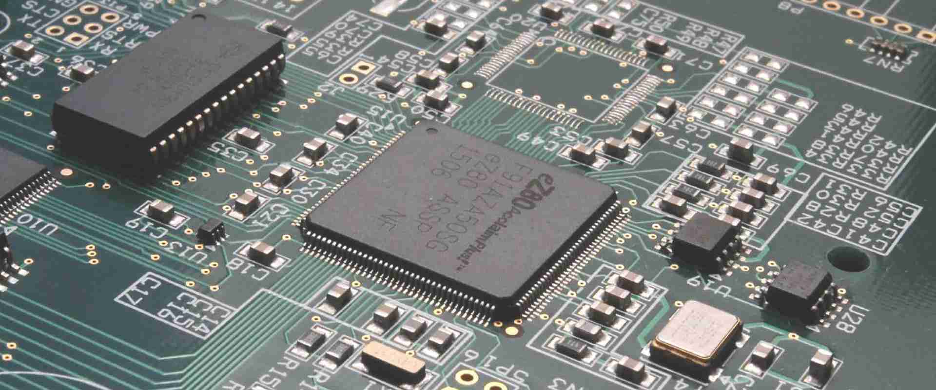
Integrated circuit (IC) transistors, diodes, resistors, and capacitors are fabricated into compact surface-level contacts configured as various SMD package styles including:
SMD Chip Components
- Rectangular or square SMD package format
- Smaller than 1.0 mm x 0.5 mm dimensions
- Includes 01005, 0201, 0402, and 0603 size codes
- Also called microchips or micro SMD parts
Flat-Leads and Gull Wing Leads
- Rectangular molded SMD component body
- Protruding leads form flat or angled wing shapes
- Enables surface gripping during assembly
- Includes SOIC, QFP, DIP chip carrier types
Quad Flat Packages (QFP)
- Square component with leads on four sides
- P pitch sizes between 0.4 mm to 1 mm
- Common with microcontrollers and logic chips
- Allows high density component placement
Ball Grid Arrays (BGAs)
- Square SMD package with grid contact balls
- Pitch dimensions from 0.5 mm up to over 2.0 mm
- Allows precision mounting of integrated circuits
- Requires solder paste reflow process
Connectors and Sockets
- Rectangular SMD card edge sockets
- USB, DVI, and memory card interconnects
- Board-to-board female pin headers
- Compact modern alternatives to DIP sockets
Table of common SMD component package styles:
| Type | Size Range | Lead Style | Example Components |
|---|---|---|---|
| SMD Chip | 01005 – 0603+ | Rectangular pads | Resistors, capacitors, transistors |
| Flat Leads | 10+ mm length | Horizontal or vertical | Op amp ICs, regulators, oscillators |
| Gull Wing | 10+ mm span | Angled away | Logical ICs, memory, microcontrollers |
| QFP | 5×5 mm – 20×20+ mm | Perimeter | Microprocessors, FPGAs, ASICs |
| BGA | 10 – 35 mm grid | Solder ball array | GPUs, complex integrated circuits |
| Connectors | 5 – 50 mm L | Edge fingers | Memory cards, board stacking |
SMD Printing and Assembly

Producing functional circuit boards with SMD components involves:
SMD Stencil Printing
- Perforated metal stencils match circuit layouts
- Deposit precise solder paste volumes
- Enable rapid automated population
Surface Mount Pick and Place
- Vacuum nozzle equipment select parts
- Transfers components onto solder pads
- Achieves very high assembly rates
Reflow Soldering Profiles
- Multi-zone ovens with thermal profiling
- Melts solder paste to electrically bond parts
- Environmentally friendly no-clean fluxes
Table showing sequence of SMD printing and reflow assembly steps:
| Step | Details | Key Factors |
|---|---|---|
| SMD Stencil | Laser cut metal | Aperture size, thickness, and pattern matching circuit layout |
| Solder Paste | Spherically alloyed mixture of tin, silver, copper | Alloy blend, flux chemistry, particle size distribution |
| SMD Placement | Vacuum pick and place | Accuracy, tip style for component package |
| Reflow Oven | Time and temperature profile | Avoid excessive time above liquidus. Peak above 183 ̊ C briefly |
| Inspection | Verify alignment, tombstoning, bridging | Process cameras, x-ray, and electrical tests |
Advantages of SMD Technology

Transitioning from insertion mounted components to surface mount devices on PCBs enables:
Miniaturization
- Extreme space optimization packing densities
- Components measured in microns
- Enables smaller and lighter end products
Performance
- Faster signal speeds with shorter traces
- High speed circuitry exceeding GHz +
- More complex component integration
Reliability
- Improved thermal heat dissipation
- Environmental protection using conformal coatings
- Reduced solder fatigue stresses
Automation
- Software design rule checking
- Volume paste print and pick & place
- Fully automated optical inspection
Serviceability
- Complete surface accessibility
- Avoid de-soldering inserted components
- Facilitates rework and repair
Table summarizing the benefits of SMD circuits versus insertion mount through hole PCBs:
| Parameter | Surface Mount | Insertion Mount |
|---|---|---|
| Size | 1/4 footprint area | Larger components, holes consume space |
| Performance | Faster speeds exceeding GHz | Limited by sockets to hundreds of MHz |
| Reliability | Vibration resistance, thermal relief | Prone to work loose over time |
| Automation | High volume compatible | Manual insertion labor |
| Serviceability | Accessible components, reworkable | De-soldering often damages PCBs |
SMD Rework and Repair
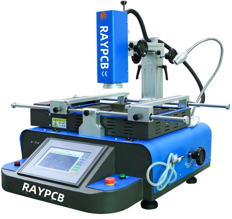
Maintaining, modifying, and repairing SMD assemblies requires specialized methods:
Benchtop Hot Air Systems
- Controllable heat blower nozzles
- Preset air temperatures up to 500°C
- Solder paste flux activation
- Multi-zone profile ramping
SMD Vacuum Pick-Up Tools
- Precise component manipulation
- Nozzle sizes match parts down to 01005
- Electrostatic dissipating models
- Flexible arm mounts optimize ergonomics
Microscope Visualization
- High magnification with ring illumination
- Stand mounting maximizes working envelope
- Cameras show magnified process indicative
- Critical for inspection and analysis
Soldering Tweezers and Irons
- Thermal tweezer construction
- Rapid temperature response
- Fine conical soldering tips
- Manageable component heat-sinking
Table listing typical SMD rework and repair equipment:
| Tool | Typical Models | Purpose |
|---|---|---|
| SMD Hot Air | Hakko FR-810, Quick 861DW+ | Blast heated air for desoldering and reflow |
| SMD Vacuum Pickup | Vastar S09 | Manipulate surface mount components |
| Microscope | Amscope 50X-1000X Zoom with boom stand | Visualize tiny chip components, solder joints |
| Soldering Iron | Hakko FX888D, MetCal MC-CS | Precise thermal transfer for re-soldering |
Frequently Asked SMD PCB Questions
How small can SMD components be on a PCB?
Industry standard 01005 chip components measure just 0.4mm x 0.2mm in size. Even smaller microchip development leverages semiconductor fabrication down to few micron scale elements and nanotechnology applications.
Is hand soldering SMD possible?
Hand soldering SMD remains realistic for prototype development, low volume production, and field repairs. This requires quality micro soldering tools, magnification, a very steady hand, and excellent technique.
How do you desolder damaged SMD components?
Removing defective parts often requires a hot air SMD rework station generating temperatures around 300°C along with vacuum pliers to lift components once joints reflow. This avoids damage uptil 600°C.
Can you wash an assembled SMD board?
PCB wash processes including ultrasonic or spray agitation risks damaging small SMT solder connections or inducing latent defects through mechanical stresses. Avoid washing finished SMD boards whenever possible.
Are lead-free solders compatible with SMD?
Yes, lead-free solders must operate around higher ~217°C melting points but work effectively for SMD assembly. They often contain mixes of tin, copper, and silver element metallic alloys combined with no clean fluxes.


