Printed circuit boards (PCBs) provide the foundation for almost every electronic device we use. Whether in phones, appliances, vehicles, or massive supercomputers, PCBs facilitate communication between components to enable complex functionality.
While often going unnoticed, the capabilities and limitations of PCB technology directly impact the size and performance of electronics. Component density, interconnects, and fabrication techniques impose key practical constraints around achieving ever-smaller PCBs.
This article will explore the extremes of miniaturization with PCBs. We’ll uncover the smallest commercially available boards today, the specialized production techniques behind them, and their applications. We’ll also glimpse the future by covering emerging methods for further reducing PCB dimensions.
What Determines PCB Size?

Before investigating extremes, let’s quickly review what generally determines the smallest feasible size for a functional printed circuit board:
Component Size and Pitch
Discrete components like resistors, capacitors, and ICs must physically fit onto the PCB surface. High-density packaging using small plastic cases and ultra-fine lead pitches enable reducing component footprint.
Trace Width and Spacing
The conductive copper traces must facilitate component connections while maintaining critical spacing rules. Narrower traces spaced closer together minimizes total area.
Fabrication Capabilities
PCB etching, drilling, and handling capabilities ultimately constrain dimensions regardless of design. We’ll explore this more below.
Application Constraints
Final device size requirements, interconnects, heat dissipation, operating conditions, and other practical aspects play a role.
With an understanding of those driving factors, let’s now investigate state-of-the-art capabilities for ultra-small PCBs.
What Are Currently the Smallest Production PCBs?
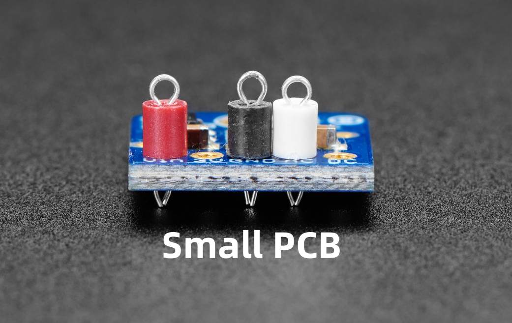
Commercially available rigid PCBs with surface-mount technology today typically range down to just 0.4mm x 0.4mm for the board substrate. This approx. 0.16 square inches area hosts traces, pads, and microscopically tiny discreet components.
For context, that is about the cross-sectional area of a single strand of human hair!
Some examples are shown below with a mechanical pencil tip for scale:
These tiny PCBs push fabrication technology to its limits while enabling applications like:
- Micro sensors
- Medical devices
- Microscopes
- Miniature cameras
- Robots
Note most production PCB houses cite 0.4mm as their lower dimension limit before etching and handling becomes infeasible. This constraint is a bottleneck for further miniaturization with conventional PCB technology.
Fabrication Considerations at Extreme Scales
Creating functional PCBs smaller than 1mm x 1mm requires specialized fabrication processes attuned to the unique material behaviors and handling requirements.
Here are some of the vital considerations:
Layer Stacking
While larger PCBs may use 6-30 conductive layers, ultra-small PCBs are generally limited to just 1-2 layers. Adding more layers compounds alignment and drilling challenges at such fine resolution.
Trace Widths and Pitches
Traces must shrink below 0.15mm width with similarly fine clearances down to under 0.1mm. This approaches the limitations of standard etching resolution and registration alignment across layers.
Via Formation
Interconnect vias between layers are impractical below 0.3mm diameter due to material filling difficulties and high aspect ratios. Their minimum spacing also rises compared to trace routing.
Component Population
01005 (0.4mm x 0.2mm) chip components help minimize footprint. But shrinking towards 008004 (0.2mm x 0.1mm) remains highly challenging with standard SMT assembly. This hampers further PCB area reductions.
Panel Thickness
Panel thickness must drop below standard 1.6mm FR-4 substrates to facilitate handling, registration, and component clearance. Thinner laminates down to 0.25mm help enable sub-1mm board sizes.
Panel Scoring and Breakout
After population, scoring tracks for singulating tiny PCBs requires precision diamond cutters. The boards are too small for typical V-scoring or routing separation methods used on larger panels. Careful handling prevents fragments or cracked components.
Pushing Below 0.4mm: Novel Approaches

While mature PCB technology bottoms out around 0.4mm x 0.4mm using the above adaptations, researchers are pioneering novel techniques to push even smaller. These emerging methods show promise for creating functional boards below 100 microns scale.
Such microscopically tiny circuit boards open doors for applications from smart dust sensors to in-body medical devices and beyond.
Here is an overview of some tiny PCB fab methods being explored:
Additive Inkjet Printing
Inkjet technology using silver nanoparticle conductive inks can “print” circuit traces and pads onto substrates. It eliminates the need for etching and enables finer resolutions below 100 microns.
Microcontact Printing
This uses a soft lithography stamping process to transfer patterns of conductive “ink” forming traces and pads. It facilitates boards smaller than 0.4mm x 0.4mm dimensions.
Flexible Kapton Films
Using thin polyimide sheets as base substrates instead of FR-4 composites helps enable microscopic via drilling and fine routing resolutions.
Chip Embedding
Entire bare IC dies get embedded into substrates using high density interconnect layers to route signals to the edges. This avoids traditional SMT packaging size constraints.
The Path Below 0.1mm PCBs
The techniques above illustrate some current capabilities to produce ~0.1mm PCB footprints accommodating simple components or modest ICs.
But there are still significant technical barriers towards enabling robust printed circuit boardssmaller than 100 microns across.
Ongoing challenges include:
- Increasing resistivity of traces below ~100nm width
- Material handling, registration, and distortions
- Heat dissipation with very low thermal conductance
- Component attachment and interconnect reliability
- economical high volume production
Innovations in materials science, additive manufacturing, nanotechnology, and assembly methods provide hope for overcoming such hurdles in the coming decades though.
The payoff will be transformative electronics seamlessly integrating into clothing fibers, into living tissue, and forming interactive smart dust permeating future megacities.
The Role of IC Chip Technology
It is worth noting that as printed circuit boards shrink towards microscopic dimensions below 0.1mm, the distinction between PCB substrate and integrated circuit begins to converge.
In essence, the foundation PCB material morphs into an extension of the IC package itself rather than a vehicle for attaching multiple discrete components.
Engineers may ultimately view and design these hybrid integrated systems using adapted IC layout tools attuned for ultra-high density lithography production techniques.
This hints at a potential paradigm shift in the way microscopic electrical systems are conceived from the board level down to the transistor level.
Summary of Smallest PCB Capabilities
To conclude, here is a breakdown of current and future tiny PCB capabilities:
| PCB Size Range | Typical Examples | Cutting-Edge Research |
|---|---|---|
| 10mm x 10mm | IoT sensors, coins cells | n/a |
| 5mm x 5mm | Microcontrollers, connectors | n/a |
| 2mm x 2mm | Medical devices, microscopes | Additive printing |
| 1mm x 1mm | Super-miniature sensors, ICs | Microcontact stamp printing |
| 0.4mm x 0.4mm | Extremely tiny discretes | Flex PCBs with embedded actives |
| 0.1mm x 0.1mm | n/a | Chip I/O interconnect approaches |
We are clearly approaching interesting inflection points in PCB and chip integration capabilities to enable the next wave of microelectronics innovation!
Conclusion and Outlook

This article explored the extremes of PCB miniaturization – tracing key technical barriers, production challenges, emerging innovations, and potential paradigm shifts on the horizon.
While physical limits prevent further shrinking boards much below 0.2mm sizes today, novel fabrication methods provide promise for pushing PCB boundaries towards truly microscopic scales beyond our imagination.
The impacts across industries like electronics, robotics, biotech, and materials science highlight why this niche domain warrants attention in coming years!
Frequently Asked Questions
How do such tiny PCBs get powered?
At microscopic dimensions below 1-2mm scale, traditional connector interfaces become impractical. Tiny boards instead leverage resonant inductive coupling, piezoelectric films, or electromagnetic harvesting to transform vibrations or ambient EM signals into usable power.
Can you solder components onto extremely small PCBs?
Soldering remains feasible down to 01005 (0.4mm x 0.2mm) sized SMD components as used on the smallest production PCBs currently. Approaching 008004 (0.2mm x 0.1mm) chip scales becomes very challenging however. Some emerging techniques utilize conductive epoxies instead of solder.
Are there size limits with semiconductor ICs as well?
Yes, shrinking IC transistor geometries and die areas face intense technical barriers below about 5nm node sizes today. Quantum and thermal effects introduce roadblocks similar to PCB scaling limits. 3D integration methods try to circumvent planar scaling challenges.
What are some application examples for microscopic PCBs?
Miniscule PCBs enable smart dust sensors, microscopic robots and drones, digital health monitoring devices, intraocular pressure sensors, ephemeral electronics, and other highly space-constrained uses.
WillConstraint PCB capabilities limit further miniaturization progress?
Emerging interconnect schemes embedded directly into microchip packaging hint at a convergence between system-on-chip ICs and traditional PCB substrate approaches. This could circumvent printed circuit board barriers in some applications.


