
Introduction
A printed circuit board or PCB forms the core foundation of all electronic circuits and products. PCBs provide the mechanical structure to mount and interconnect electronic components using conductive copper traces etched on an insulating substrate. Based on their structure, PCBs can be classified as single sided, double sided or multilayer.
This article provides an in-depth understanding of what single sided PCBs are, their properties, manufacturing processes, applications and comparisons with double sided boards.
What is a Single Sided PCB?
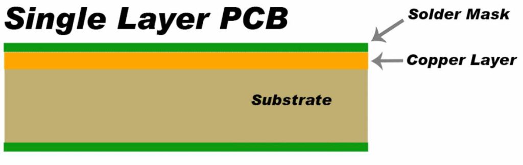
A single sided PCB has the copper circuit pattern only on one side of the insulating dielectric base material. The components are mounted and soldered onto the same side containing the conducting tracks. Vias or plated through holes are used to establish connectivity between the top conductive layer and the bottom soldering side.
Some key characteristics of single sided PCBs:
- The circuit pattern is on only one side of the dielectric substrate.
- No internal buried signal layers. External components populate one side.
- Holes are drilled and plated to form vias for vertical interconnections.
- Used in simple, low component density circuits like basic electronics projects.
- Cheaper to manufacture compared to double sided and multilayer PCBs.
- Maximum PCB size is dictated by fabrication equipment capability.
- Board thickness ranges from 0.4mm to 3.2mm based on copper weight and material.
- Common materials used are FR-4 glass epoxy, CEM, PTFE, Polyimide, etc.
Properties of Single Sided PCBs
Single sided PCBs have the following typical properties:
Dielectric Substrate
- Materials like FR-4 (glass fabric reinforced epoxy), CEM-1, Polyimide, PTFE Teflon etc.
- Thickness – 0.2mm to 3.2mm
- Copper clad on one or both sides
Copper Thickness
- 1 oz (35 μm) or 0.5 oz (18 μm) generally
- Thicker 2 oz (70 μm) also possible
Minimum Track/Spacing
- ~6 mil (0.15mm) lines and spaces
Hole Sizes
- 0.3mm to 2.5mm standard range
- Microvias down to 0.15mm possible
Soldermask and Silkscreen
- Green soldermask on both sides
- White silkscreen for component designators
Plating
- Hasmetallization in holes to form vias
- Hot air solder leveling (HASL) finish mostly
- Immersion silver, ENIG also possible
Common Sizes
- Small – 25mm x 25mm to 160mm x 100mm
- Medium – 160mm x 233mm
- Large – 457mm x 610mm
Manufacturing Process Steps
Single sided PCBs are fabricated using the following sequence of steps:
1. Copper Clad Laminate Preparation
- Raw dielectric substrate is cladded with copper foil on one or both sides.
- FR-4 glass epoxy is commonly used. Other options are polyimide, PTFE, etc.
2. Drilling
- Tooling holes are drilled first for alignment followed by holes for vias or component mounting.
3. Photolithography
- Photosensitive film dry resist is laminated on copper surface.
- Desired circuit pattern is exposed using UV light.
- Resist from unexposed areas is washed away chemically.
4. Copper Etching
- Unwanted copper without resist is etched away leaving required tracks.
- Most common method used is chemical etching.
5. Photoresist Stripping
- After etching, the remaining photoresist dry film is stripped away.
6. Hole Plating
- Copper is plated onto inner walls of drilled holes to form conductive vias.
7. Soldermask Application
- Epoxy based soldermask is screen printed on both sides leaving exposed pads.
8. Silkscreen Printing
- Component designators, logos, markings are printed for identification.
9. Surface Finish
- HASL, immersion silver, gold plating or OSP finish is applied on exposed copper.
10. Electrical Testing
- Continuity, isolation testing is conducted before shipment.
Typical Applications
Some typical applications where single sided PCBs are commonly used:
- Simple analog and digital circuits
- Basic electronic projects and hobbyist boards
- Educational training kits
- Toaster, rice cooker, induction cooker, blender type appliances
- LED lighting fixtures and ballasts
- Power supplies, UPS systems
- HVAC and building automation systems
- Simple industrial automation modules
- Basic instrumentation
Where component density is low and routing is not complex, single sided boards provide a cost effective solution compared to double sided boards.
Comparison Between Single Sided and Double Sided PCBs
Here is a comparison of key differences between single sided and double sided PCBs:
| Parameter | Single Sided PCB | Double Sided PCB |
|---|---|---|
| Circuit layers | One conductive layer | Two conductive layers – top and bottom |
| Component placement | On one side only | Both sides |
| Track routing | Limited, longer routes | Much better, shorter |
| Component density | Low density circuits | Higher density packing |
| Manufacturing cost | Lower | Higher due to more process steps |
| Circuit complexity | Simple circuits | Complex, dense circuits possible |
| Weight | Lower | Higher due to double sided lamination |
| Common applications | Basic electronics, appliances | Computer motherboards, communications |
Pros and Cons
Advantages of Single Sided PCBs
- Cheaper and simpler to manufacture
- Low material cost
- Quicker delivery
- Suitable for simple, low-density circuits
- Easier repair and rework
Disadvantages of Single Sided PCBs
- Limited board space as components only on one side
- Restricted component placement
- Longer copper track routing
- Not suitable for complex, dense circuit layouts
- Limited to low frequency, low power applications
Frequently Asked Questions
Q: What are the different types of PCBs?
A: The main types of PCBs based on layer structure are:
- Single sided – Conductors on one side
- Double sided – Conductors on both sides
- Multilayer – Three or more conductive layers
Q: What are vias in PCBs?
A: Vias are plated through holes in PCBs that provide electrical connectivity between layers to route signals across both sides.
Q: What are the typical substrate materials used in PCBs?
A: Common materials are FR-4 glass epoxy, CEM-1, Polyimide, PTFE, Rogers laminates, Arlon, Nelco etc. FR-4 is the most popular.
Q: What are the different PCB fabrication processes?
A: Main processes are etching, drilling, plating, soldermasking, silkscreen printing. Advanced methods like laser drilling, photolithography are also used.
Q: What are the typical finishes used on PCBs?
A: Common finishes include HASL (tin-lead or lead-free), immersion gold, immersion silver, OSP, ENIG to protect copper traces from oxidation.


