A single sided PCB (printed circuit board) contains conductive copper traces patterned on only one side of the base dielectric substrate material. All components and routing reside on the same top layer surface.
Single sided boards provide an affordable option for simple circuits not needing complex interconnects or multilayer stacking. Applications range from basic lighting fixtures or toys up to some control boards and analog/radio frequency designs.
This article provides a detailed overview of single sided PCB capabilities, technologies, design considerations, manufacturing processes, and costs implications relative to more complex multilayer boards.
We’ll also cover limitations posed by single layer boards and criteria around when opting for multilayer may become necessary.
Key Characteristics
Below are the core attributes defining single sided PCBs:
Single Conductive Layer
All conductive copper traces reside on the same outer surface of the board. Additional internal buried or blind layers are not utilized. This simplifies layout.
Double-Sided Component Placement
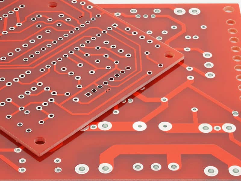
While only one side hosts tracings, components occupy both top and bottom sides of a single sided board. This maximizes surface utilization.
Single Sided Board with Traces and Components on Both Planar Surfaces
Plated Through Hole (PTH) Interconnects
Since no internal layers exist, traces cannot run within the PCB. Instead, plated through holes provide connections between top and bottom sides when routing is needed between the two planes.
Limited Interconnect Density
With a single conductive layer and all routing sharing the same surface, intricate cabling between many closely spaced components becomes challenging. This hampers interconnectivity density.
Lower Performance Thresholds
Electrical characteristics such as high frequency signaling, fast logic timing, tightly regulated power distribution, and precision impedance control suffer relative to boards with multiple reference plane layers.
In light of these innate characteristics, single sided PCBs naturally suit less complex circuits.
Manufacturing and Fabrication
Single sided boards utilize similar core fabrication processes as more complex multilayer types but with notable simplifications:
Board Materials
Typical low-cost FR-4 glass epoxy composites serve well for single sided substrates since dielectric consistency largely doesn’t impact performance. Some variants include:
- Standard FR-4 – Well proven, moderately temperature tolerant
- High-Tg FR-4 – Improved thermal rating for lead-free soldering
- CEM-1 – Superior thermal performance but costlier
- Polyimide – High puncture resistance for thin flexible boards
Layer Alignment
Only the outer copper layer needs patterning on single sided PCBs. This avoids complex layer-to-layer registration and vertical interconnect challenges during lithographic imaging and etching of buried sublayers.
Route Planning
With no internal layers, all connectivity must occupy the same set of x-y routing channels. This pressures designers to mind component placement judiciously. Longer trace lengths degrade signal performance in some circuits.
Via Formation
Drilled and plated through hole (PTH) vias can readily connect top and bottom reference planes as needed. But skip PTH whenever possible to reduce cost. Blind and buried vias do not apply since no internal layers exist.
Testing and QA
With only one active conductive layer, inspecting assembly and quality requires simpler visual auditing. This contrasts more intricate buried sublayer checks needed for multilayer boards during fabrication.
Design and Layout Considerations
To leverage their singular layer effectively in circuit implementation, certain principles guide single sided PCB layouts:
Component Placement
Group associated circuit sections intelligently to minimize interconnect distances between related functional blocks. Claude components needing tight couplings or timing together dutifully.
Localized Power Distribution
Distribute power supply rails beneath respective load components using wide supply traces or polygon pours. This limits voltage drop over long thin traces back to sources.
Mixed Signal Routing
Keep analog signal chains physically separated from nearby digital lines or switch-mode supplies to avoid coupling noise onto sensitive nodes.
Crossing Management
Route wires orthogonally when crossing to avoid unintended capacitance. Narrower traces help further minimize capacitive coupling between perpendicular signal lines.
High Frequency Considerations
Use larger clearance gaps between traces, guard ring polygons, and aggressive staircase routing when dealing with radio frequency (RF) circuits. This enhances electromagnetic isolation.
Heat Management
Carefully position heat-sensitive components away from large power devices or transformers that dissipate significant warmth. Thermal dissipation options remain limited on single layer boards.
While requiring some adaptation from multilayer conventions, single sided boards do provide enough practical routing density for many cost-sensitive applications when following design practices like the above.
Comparing Single Sided vs Double Sided PCBs
Upgrading from a single copper layer PCB to double sided alternatively allows partitioning routings across two conductive planes. This helps alleviate layout congestion, but still lacks multilayer flexibility.
Single Sided Pros
- Simpler layout
- Lower fabrication cost
- Acceptable for uncluttered circuits
Double Sided Pros
- Double the routing capacity
- Components on both sides
- Improved planar utilization
- Lower congestion
In essence, double sided PCBs provide incremental enhancements over single sided but retain similar expressly planar architectures.
Cost sits between single and multilayer boards while accommodating moderately more complex component arrangements.
Limitations and Shift Towards Multilayer
While useful within constrained applications, single PCB layer inherently restricts circuit intricacy due to routing congestion since no internal layers exist. This drives several limitations:
Density and Complexity Walls
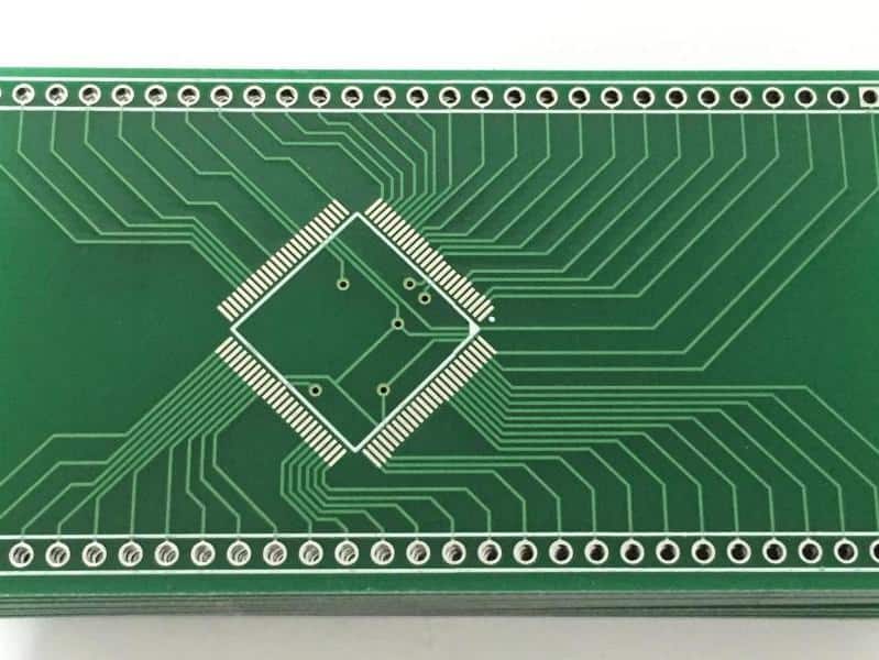
Intertwining connectivity between numerous components becomes impractical beyond a certain point. Large IC pinouts also become problematic given finite routing channels.
Electrical Performance Ceilings
With no internal reference planes for encapsulating signals, characteristics like crosstalk, reflection noise, and EMI radiation degrade. Controlled impedance environments also cannot be achieved.
Manufacturability Challenges
Extreme component densities strain fabrication capabilities and solder mask coverage since everything shares the same planar surface area. Reaching production yield targets grows difficult.
Economic Inefficiency
As operating frequencies, power levels, functional sophistication levels, and bandwidth demands all scale up, single sided boards burn disproportionate planar real estate. This wastes board space which raises end-product costs.
In light of the above hurdles, the industry migrated towards multilayer PCB architectures for the majority of applications.
Multilayer PCB Comparison
Modern complex PCBs with 4+ layers alleviate many single sided limitations for advanced electronics through:
More Routing Layers
Stacking several conductive copper layers with intermediary insulating dielectric substrates provides multiples more routing capacity. High speed signals route on inner layers.
Blind and Buried Vias
Vertical interconnects thread signals between layers without consuming space on outer surfaces. This greatly expands wiring options.
Reference/Ground Planes
Continuous power and ground planes encapsulate signals preventing external noise coupling or emissions leakage. Controlled impedance environments also result.
Higher Component Densities
Components occupy mainly the outer surfaces while traces tunnel through layers internally. This intensifies overall packing densities while separating conflicting signals.
Superior High-Speed Performance
Careful layer stacking, planes removal of crossing, impedance control, and risk reduction from tighter electronics integration.
In light of those benefits, few PCB use cases remain where single sided implementations still suffice given contemporary electronics capabilities.
Contemporary Usage Cases

Which applications still leverage single sided boards despite the multilayer dominance trend? Some areas include:
Cost-Sensitive Products
Toys, basic appliances, lighting fixtures, and hobbyist experiments prize affordability over complexity. This sustains some single layer demand.
Power and Analog Circuits
Isolated converters, power electronics, or analog signal conditioning sometimes avoid multilayer costs given modest complexity needs.
Radio Frequency PCBs
Surprisingly, some RF designs like filters, antennas, couplers, and barebones control logic exploit single sided quartz or ceramic substrates for optimal RF performance.
High Voltage Boards
The intrinsic layer-to-layer weaknesses and thicker dielectrics of multilayer boards make tuning them for ultra-high voltage applications difficult.
Quick-Turn Prototyping
Rapid board fabrication turns benefit from only processing a single conductive layer to validate concepts before final multilayer migration.
While exceeding scarce, these technology areas help single sided PCBs cling onto limited lingering niche relevance despite clear long-run declines.
Conclusion
In summary, we’ve explored single sided printed circuit boards constituting the most basic variety with conductive traces and connectivity residing solely on one external substrate facet.
We covered their distinct traits, associated layout considerations, comparative manufacturing simplicity, inherent performance and density limits prompting multilayer adoption, and where some fringe vestigial applications still leverage single sided designs today despite limitations.
This foundation helps contextualize their place within the broader PCB technology universe spanning everything from rudimentary single layer boards to complex high-density multilayer marvels housing millions of components operating at blinding frequencies.
Understanding the spectrum of PCB platforms in terms of capabilities, costs, electrical characteristics, fabrication considerations and applications delivers crucial perspective across electrical engineering domains touching electronics hardware.
Hopefully this breakdown of legacy yet still relevant single sided boards provides useful insight into PCB technological ecosystems!
Single Sided PCB FAQs
What are some key differences between single sided vs double sided PCBs?
Double sided boards upgrade from one to two external conductive layers. This doubles routing capacity since traces can fully utilize both top and bottom sides rather than just one. Through-hole interconnects remain necessary between layers.
Do single sided PCBs have any internal copper layers?
No, true single sided boards only have the one external conductive layer on a single substrate facet. No additional buried or blind layers exist internally. Double sided enhances to two external layers while multilayer has 4+ total conductive layers.
What are limitations of single sided PCB technology?
Routing congestion arises rapidly given finite board area. This constrains complex connectivity between many dense components also populating the same surfaces. Performance further degrades sans impedance control or encapsulation reference planes between signals.
What PCB technology superseded single sided boards?
Multilayer PCBs with 4+ stacked conductor layers interconnected through high-density plated vias/holes largely displaced single sides boards to achieve vastly greater complexity, performance, and integration economies. Some niche single sided uses remain.
Are there any modern electronics applications still leveraging single layer PCBs?
Yes, cost-sensitive products like basic appliances, RF analog boards, high voltage systems, and rapid prototyping still utilize them. But for intricate digital functionality, multilayers now dominate across computing, telecom, automotive, industrial, and nearly all sophisticated electronics.


