Printed circuit boards (PCBs) form the core foundation of electronics hardware providing the platform for mounting components and interconnecting them. As applications spanning computing, communications, healthcare, automotive etc continue to get complex, PCB technology is evolving in tandem.
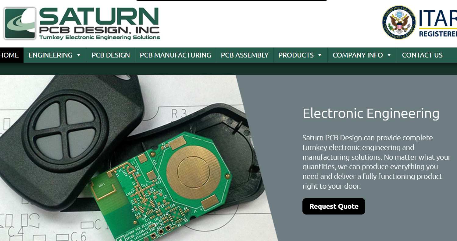
Saturn PCB refers to a novel 3D fabrication approach intended to offer next generation multi-functional performance beyond conventional 2D PCB structures.
This articles covers Saturn PCB architecture including:
- Motivation and comparison to existing PCB technologies
- Working principles and 3D fabrication methodology overview
- Applications landscape where Saturn PCBs offer benefits
- Industry ecosystem status and future outlook
By the end, you would gain insights into this futuristic PCB technology along with its differentiation relative to widespread FR4 boards.
Limitations of Conventional 2D Printed Circuit Boards

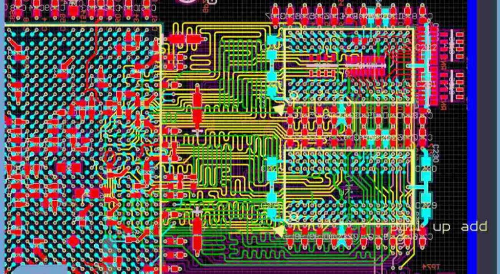
Traditional rigid or flexible PCBs rely on printing thinly layered sheets of laminates like FR4 material to achieve interconnections between mounted components. As electronics functionality grows more complex and compact, inherent drawbacks of planar PCBs arise involving:
- Routing congestion with 2D space constraints limiting interconnections
- Thermal rise issues due to absence of heat dissipation avenues
- Impedance mismatches and signal integrity challenges
- Limited modularity and post fabrication integration capability
- Scaling barriers for mixing components of varied dimensions
This necessitates reinvention of foundational board technology itself to address constraints. And Saturn PCB offers promising 3D fabrication methodology overcoming above factors as discussed next.
Introducing Saturn PCB Technology
Saturn PCB refers to an advanced 3D printing inspired “stacked cubes” architecture for embedding electronics functionality.
The key highlights of Saturn technology include:
- Proprietary 3D printing process allowing multi-axis interconnections
- Enables mixing components of dissimilar sizes like ICs, capacitors, resistors together through adaptive placement
- Integrated heat extraction pathways by leveraging interior routing channels
- Embedded cuboids structure aids concurrent multi-signal routing through vertical facets
- Component-less soldering process ensures reliability through high precision fabrication
- Modular assembly methodology supports scalability and reconfiguration
Thereby Saturn PCB offers next generation multi-functional performance to meet increasingly complex application requirements over traditional planar circuit boards.
Working Principle
The Saturn PCB architecture relies on an innovative multi-axis routing methodology through its 3D cube synthesis process capable of interconnecting conventional electronic components in unconventional modes.
The technologies involved can be functionally decomposed into:
1. Design and Simulation
Proprietary EDA software allows predictive modeling and analysis of target functional configuration based on multi-axis routing considering electronic, thermal and mechanical boundary conditions. Critical pre-fabrication validation happens through simulation.
2. Fabrication
A hybrid micro-scale manufacturing system synthesizes the electronic cubes assembly leveraging cutting edge 3D micro-printing process aided by robotic component integration and advanced metrology feedback.
The core steps include:
- Material deposition
- Micro-machining
- Component embedding
- Strut formation
- Surface finishing
The repeatable process ensures consistency and reliability required for electronics manufacturing.
3. Validation and Testing
Prior to deployment, Saturn modules undergo comprehensive signal integrity, power integrity and functional validation leveraging laboratory grade instrumentations. System level assessment combined with early stage modeling minimizes field issues.
4. Applications Assembly
Finally, the modular Saturn PCB cubes get integrated into target platforms through structural attachments and electrical bonding to external interfaces or peripherals as dictated by project needs.
Thereby through fusion of design, manufacturing and integration techniques, the holistic Saturn technology tries addressing limitations posed by prevalent 2D printed circuit boards.
Benefits over Conventional PCBs
Comparing Saturn 3D boards to prevalent rigid/flex 2D PCBs, below differentiation areas arise:
| Conventional 2D PCBs | Saturn PCB | |
|---|---|---|
| Design Approach | Planar | Multi-axis 3D structure |
| Routing Layers | Limited to conductor layers in 2D | Multi-directional interconnections |
| Heat Dissipation | Constrained without heat spreading options | Integrated cooling struts |
| Heterogeneous Integration | Mostly uniform components sizes | Adaptable embedding of varied dimensions |
| Signal Quality | Having SI, EMI and PI issues | Careful modeling minimizes distortions |
| Fabrication Process | Subtractive printing methods | Additive manufacturing technology |
| Scalability | Redesign needs for changes | Module based assembly enables alterations |
| Post Production Rework | Manual, risky for miniature components | Reconstruction flexibility through modularity |
Thus the 3D Saturn architecture tries overcoming limitations posed by single plane fabrications.
Multiple industry collaborations are underway to leverage Saturn PCBs across applications from aerospace to servers for reforming electronic systems fabrication and integration.
Applications Landscape

Given its multi-functional attributes, Saturn PCB technology becomes extremely versatile addressing needs across domains:
A. High Performance Computing
- Next generation data center, HPC and cloud installations
- Hardware accelerated AI and ML training platforms
- Low latency switched architectures
B. Defense and Aerospace
- Radars, sensors, guidance systems etc.
- Avionics distributed control systems
- Rugged electronics for harsh environment tolerance
C. Medicine and Healthcare
- Implants, wearables and diagnostics
- Lab automation instruments
- Miniaturized surgical devices
D. Automotive Systems
- Autonomous driving assistance and control functions
- Battery management and EV powertrain
- Advanced driver assistance systems (ADAS)
E. Energy
- Motor controllers for white goods and UAVs
- Smart grid electronics
- Renewables integration and microgrid development
With exponential advancements in underlying semiconductors, the role of interconnection medium becomes pivotal in unlocking their usable potential. And Saturn PCB offers such transformative platform through its 3D fabrication methodology meeting demands of emerging applications.
Industry Status and Developments
While still in stages of industrialization, Saturn PCB is seeing increased experimentation and early adoption traction:
- Materials and fabrication equipment partners focusing to enhance repeatability and scale
- EDA vendors extending modeling capabilities for concurrent thermal-electrical simulations
- Research publications demonstrating multi-physics analysis targeted for reliability
- Electronics manufacturers evaluating for integration into aerospace and defense projects
Additionally industry consortiums are formed to proliferate common understanding and set standards. For instance, groups like IPC Saturn PCB committee are working towards specifications covering:
- Materials and performance ASME standards
- Supply chain control protocols
- Reference architecture illustrations
- Manufacturing guidance including design, assembly and inspection
Such industry wide engagements will gradually help Saturn PCB adoption both for high reliability applications and accelerate mainstream hardware development leveraging 3D multi-axis routing capabilities.
Future Outlook
According to market researchers and industry specialists, Saturn PCB is expected to expand applications footprint gaining double digit CAGR traction over the next decade spanning:
- Next generation electronics applications requiring complex compact multi layered PCB structures which becomes realizable through Saturn’s conformal advantages
- High throughput computing infrastructure for HPC data centers that need to optimize space, thermal and latency parameters simultaneously
- Aerospace and defense equipment subject to extreme space, weight and harsh environment constraints
- Advent of embedded AI requiring optimized training and inference platforms simultaneously
- Connected mobility systems including automotive drivetrains, battery management predicated on signal and power integrity
- Exponential rise across IoT and edge nodes requiring fail-safe local processing
Thereby the Saturn proposition covering electrical, mechanical and thermal attributes holistically seems poised to transform future electronics packing across miniaturized to high performance segments in the long run.
Frequently Asked Questions
Q1. What is Saturn PCB technology and what problems does it seek to address?
Saturn PCB refers to an advanced 3D printing inspired fabrication approach for electronics interconnection overcoming limitations like thermal rise, routing congestion, integration challenges associated with conventional planar 2D printed circuit boards.
Q2. What are the typical application areas where Saturn PCBs offer most benefits?
Some domains where Saturn multi-axis routing and modular assembly brings discernible advantages involve aerospace systems, healthcare instruments, data center computing, defense electronics and automotive components subject to combined space, performance constraints.
Q3. What is the current industry status for Saturn PCB technology adoption?
While still maturing, Saturn PCB development is seeing increased private funding and sectoral consortiums formed indicating promising outlook. Gradual adoption is underway through pilot projects in aerospace along with various supply chain tooling aspects being standardized by groups like IPC.
Q4. What are the future projections for Saturn PCB production at commercial scale?
According to researchers, Saturn PCB fabrication techniques would get proliferated for volume manufacturing within next 3-5 years timeframe spanning applications from mainstream consumer electronics to specialized industrial equipment as complexity, miniaturization continues unabated powered by underlying semiconductor advances.
Q5. How does Saturn PCB fabrication methodology vary from conventional PCB printing techniques?
Instead of planar layer by layer 2D printing approach, Saturn leverages additive 3D micro-printing process allowing unconventional multi-axis interconnections between components shaped as cubes/blocks thereby overcoming packing density, thermal, and heterogeneous integration issues associated with prevailing rigid/flex PCB technologies.


