A right angle PCB right angle pcb allows mounting daughter cards and mezzanine modules perpendicular relative to a main printed circuit board (PCB) such as server motherboard or a backplane using special right-angled connectors. This arrangement saves space in crowded electronic enclosures by stacking boards vertically while retaining front access to I/O ports.
Right angle architectures have become a necessity in modern board layouts due to progressive miniaturization. This article will provide a comprehensive overview of PCB right angle interconnection approaches examining definitions, connector/fabrication considerations, implementation guidelines plus pros and cons to aide design decision making.
What is Meant by Right Angle PCB?
A right angle PCB configuration contains the main PCB oriented horizontally hosting various logic, power and interface components. A secondary PCB is then mounted vertically either along system enclosure edges or on raised card guides through electromechanical connectors routed from bottom side on the main board.
This allows positioning of peripheral modules like fans, I/O adapters, graphics/accelerator cards perpendicular to motherboard by connecting through underlying right angled socket strip. Top side of motherboard remains clear for access rather than being blocked by mezzanine PCBs oriented parallel to it.
Some terminology used in context of right angle PCB connectors include:
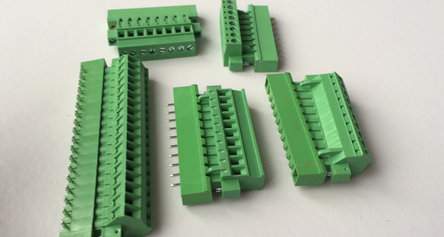
Daughter Card: The secondary smaller PCB mounted vertically hosting peripheral functions. Also called mezzanine card.
Header: Plated pin receptacle soldered to motherboard interfacing with daughter card module. Provides both electrical connectivity and mechanical alignment.
Socket Strip: Molded housing with pins that solders to daughter card with pins mating with receptacle header on main board.
Above right angle mounting scheme saves enclosure rack space with cleaner layout separating core computing cards from peripheral modules in networking/telecom/industrial hardware.
Manufacturing Approaches for Right Angle Attachment

There are three fundamental approaches provided by PCB manufacturers for implementing right angle board connections:
1. Discrete Wires or Cables
Uses individual hookup wires soldered between boards requiring significant effort. Provides flexibility but not robust mechanical stability.
2. Rigid Board Stacks
Joins PCBs together through rigid connector pairs. Gives ruggedness at expense of serviceability needing full disassembly for updates.
3. Compliant Interposers
Intermediate flexible circuit membrane placed between boards having fingers on both sides provides compliant vertical offset allowing servicing.
Above options cater to varied density, the replacement needs balanced by product lifecycle constraints helping optimize manufacturing goals.
Comparison of Right Angle Joining Methods
| Approach | Pros | Cons |
|---|---|---|
| Cables | Adjustable | Tedious process |
| No PCB changes | Unreliable mechanical rigidity | |
| Board Stacks | Rugged | Labour intensive for upgrades |
| Good signal integrity | Re-work challenges | |
| Interposers | Compliant vertical offset | Extra component – reliability risk |
| Allows easy replacement | Costlier process |
Table 1: Comparison of Right Angle PCB Attachment Approaches
Interposers using flexible circuits attempt bridging best across above trade-offs between simplicity, reliability and serviceability factors.
Right Angle Connector Types
Electrical interfacing from motherboard to daughter card is enabled by two classes of board to board right angle connectors:
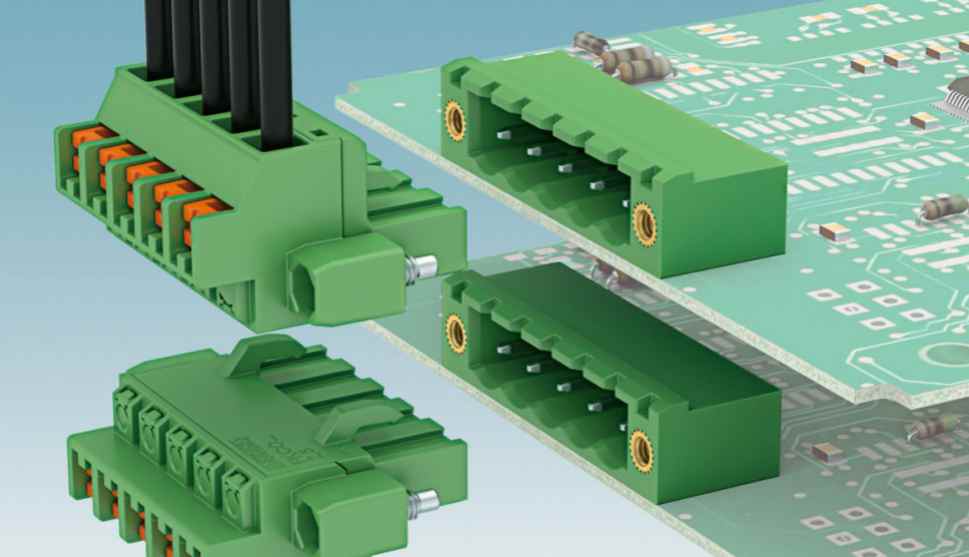
1. Female Receptacle Headers
These connector sockets gets soldered to motherboard on bottom side with vertical pins extending as anchoring points for peripheral module. Pitch sizes range from 1 to 5 mm with tunnels allowing other components underneath. Provides flexibility for mixing mezzanine cards.
2. Male Pin Strips
PCB edge fingers extensions having plated through holes matching header pin pitches. Soldered to daughtercard module directly plugging into bottom side female receptacle achieving mechanical stack. Some variants allow hot swappable insertion/removal without needing header de-soldering.
Above connector pairing supports the 90 degree interfacing allowing configurability plus replaceability crucial for demanding applications like hardware accelerated AI requiring frequent upgrades.
Next we examine popular header form factors and socket strip variants.
Right Angle Header Types
Industry standard header options to implement female receptacle on motherboard include:
1. Single Row Female Headers
Most common linear format usually along board edges having a single line of contacts accepting male pin strip insertion from daughtercard above. Pitch ranges from 1 mm allowing high density to 2.54 mm or more for ruggedized power versions.
2. Dual Row Female Headers
Contain pairs of rows with tunneled contacts allowing escape routing in between. Provides high contact density in compact width footprint. Common for stacking memory DIMMs.
3. Rectangular Matrix Headers
Grid array female receptacles with multiple rows and columns spanning area underneath daughter card zone allowing area connectivity rather than just edge mounting. Used where wider interface needed.
4. Mixed Layout Headers
Combination headers with power pins segregated from signals allowing isolation plus retention of modular replaceability. Typical for power hungry daughtercards.
So in addition to pitch, connectivity layout is an important header selection factor based on interface needs allowing optimization.
Right Angle Pin Strips Styles
Common connector pin strips soldered to periphery of daughtercard to mate with underlying receptacle headers include:
1. Straight Solid Pin Strips
Rugged right angle pins for through hole soldering. Simple and reliable but may need header de-soldering for replacement. Used for basic peripheral cards.
2. Angled Retention Clips Strip
Pins right angle tuned for header mating but ends have spring clips allowing card retention without soldering. Permits card hot swapping satisfying servicing needs.
3. Staggered Dual Row Angled Pins
Pins placed offset allowing high density routing escaping on daughter card layer underneath. Caters to complex layer escape via floorplanning on performance cards.
4. Guide Pin Strip
Has elongated guide tabs for polarization, additional pegs assisting card seating aided by visual notch keys. Used for missions critical slots prone to human errors.
As evident, both header receptacles and pin strips allow optimization across density, servicing, polarization or routing considerations as demanded fit to purpose.
Right Angle Connector Materials and Finishes
A right angle board to board interconnection undergoes wear and tear requiring choice of robust materials finishing. This spans across pins, housings, latches etc:
Header Housing Materials
- Thermoset plastics (PPA, PPS, LCP)
- Plastics with mineral or glass fill for preventing wear
- High temperature grades for rugged duty
Pin Materials
- Copper Alloys (Phosphor bronze, beryllium copper)
- Stainless steel pins for corrosion resistance
Plating Choices
- Tin for cost effectiveness
- Gold over Nickel under plating for reliability
- Selective platings like Gold tips for contact zone wear prevention
Material selection is thus an important criterion for connector optimization targeting performance longevity matching application duty cycle over service lifetime spanning years.
We next examine some implementation guidelines driving architecture and layout.
Guidelines for Right Angle PCB Layout
Here are some key guidelines when incorporating right angle board to board connectivity laying out PCB:
1. Placement Height: Define height of daughter card from main PCB surface using standoffs allowing clearance for tallest components underneath avoiding collisions plus sufficient card removal/insertion clearances.
2. Contact Density: Determine signal/power connectivity needs driving header contact count and respective pin strip widths. Dense signal traces need finer 1 mm pitch while power lines suit 2.54 mm or more.
3. Escape Routing: Plan bottom side inner layer stackup with sufficient layers to escape dense pin header arrays without excessive vias allowing isolation over signal return paths. Relevant for high speed digital links.
4. Polarization: Implement asymmetric chamfered card edges with matching receptacle notch and keys preventing incorrect daughtercard orientations. Vital for PCIe, DRAM, network daughtercards.
5. Card Retention: Specify additional latching, ejectors, extractors based on retention force requirements determined through vibration testing preventing dislodge. Important for mission critical applications.
6. Strain Relief: Anchor bulky cables exiting card using ties downs avoiding vertical yanking loads transmitted to solder joints preventing intermittent signal faults over service loads and vibration exposure.
Getting above interconnect implementation details right the first time itself helps mitigate costly redesign churn impacting schedule during later stages.
We next examine manufacturing and assembly considerations for right angled daughtercards and respective interconnects.
Manufacturing Right Angle Boards
Specialized PCB fabrication approaches needed for right angle boards include:
1. Impedance Control
Maintain differential pair impedance tolerance across right angle bends through neck-downs or back-drills plus symmetry between length tuning structures on main and daughter cards keeping signals clean.
2. Layer Transitions
Plan layer buildup placing reference ground layers adjacent to each other during 90 degree routing path transitions for shielding signal conductors from underlying digital noise sources preventing signal corruption.
3. Structural Ribs
Incorporate metallic ribs running along the right-angle height edge for rigidity preventing daughter card bending under shock, vibration conditions maintaining connector mating integrity and preventing intermittent faults.
4. Contact Plating
Use connector contacts allowing 30 micro-inch or heavier gold plating with nickel underlayer over copper pins catering to 10K+ insertion cycles without increasing contact resistance and signal failures over service life.
By proactively addressing fabrication and assembly issues upfront through such design guidelines allows smooth manufacturing release and field deployment gains.
Advantages of Right Angle Architectures
Some benefits offered by right angle PCB configurations include:
1. Space Savings
Orthogonal board placement save enclosure depth with peripheral cards stacked vertically separated from main board layout hosting processors and memory slots. Allows better airflow as well in servers.
2. Accessibility
Keeps motherboard I/O interface ports accessible from front rather than blocked by mezzanine PCBs needing cabling routed to backplane improving serviceability.
3. Signal Integrity
Short vertical interconnects allow retention of signal quality using impedance tuned routing traces, ground guards minimizing external noise interference crucial for PCIe Gen 4, HDMI 2 speeds.
4. Configurability
Mix of common headers allows changing combination of peripheral daughter cards not affecting main computing modules catering to emerging AI, machine learning hardware needing upgrades.
There are however certain limitations as well discussed next.
Limitations of Using Right Angle Scheme
Few concerns associated with right angle architectures include:
1. Exposure to Shock and Vibration
Cantilevered daughtercards with heavy protruding add-on cards subject to failures under sustained shock and vibration environments requiring additional card locks.
2. Thermal Loads
Peripheral cards stacked close together pose device cooling challenges requiring lateral air flow or dedicated heat sinks for each card preventing thermal throttling.
3. Fabrication Complexity
Need for impedance control layers, reference plane placement plus structural reinforcements increase board fabrication costs requiring volume scale to amortize NRE expenses.
4. Compliance Testing
Validation testing needed covering diverse insertion cycling, drop shock, thermal soaks adding to cost for cover mission critical daughtercard slots like graphics cards.
While above concerns can be mitigated through design analysis plus testing – make vs buy economics need evaluation vis-a-vis application constraints.
Summary
Right angle PCB configurations serve an important role allowing daughtercard partitioning in space constrained enclosures. Using appropriate connector schemes combined with fabricated stackup optimization enables reliable system integration addressing next generation hardware upgrade needs.
Getting proper implementation guidance validated upfront lowers manufacturing risks allowing deployment success in demanding environments. With increasing focus on impeccable signal quality plus equipment serviceability – right angle scheme adoption provides an advantageous edge complementing function needs.
Frequently Asked Questions
Q1. Why use right angle PCBs instead of riser cards?
Right angle PCB scheme allows short trace routing ideal for multi-gigabit speeds unlike long riser cables. It provides firm board locking unlike slots. Configuration diversity by mixing headers catering to evolving data center needs.
Q2. What drives adoption of right angle architectures?
Need for space savings by orthogonal placement combined with accessibility needs is fueling adoption to pack more functionality in compact volumes. Interface speeds needing tight impedance control also benefit through right angle schemes.
Q3. What connector pin pitch sizes are most common?
1 mm pitch connectors allow high density I/O applications like chiplet integration modules requiring many signals interconnects while 2.54mm better suits rugged power delivery applications demanding higher current capacity has tradeoff.
Q4. What validation testing is recommended?
Segment level drop shock per IEC standards, vibration endurance trials per telco specs at the interconnect areas confirms reliability. Signal integrity measurements using TDR scans, eye diagrams under long term temperature soaks ensures integrity underuse conditions.
Q5. What fabrication technology builds right angle boards?
Right angle boards demand tight impedance control of traces undergoing 90 degree bends hence processes like Tachyon allowing precise etching suited over standard quickturn board shops plying uniform trace widths unable to meet exacting electrical needs.


