With constant technology innovation and upgrade cycles measured often in just a few years, a massive tide of electronic waste accumulates as older devices get replaced by newer, faster generations. Printed circuit boards (PCBs) packed with intricate copper interconnects, difficult-to-mine precious metals, and potentially hazardous materials lie at the heart of nearly every discarded smart gadget or appliance.
So considering massive volumes, can circuit boards be recycled sustainably – or are they destined for landfills threatening health and environmental damage?
If properly implemented, responsible PCB recycling and reclamation processes not only mitigate ecological harm, but also transform end-of-life electronics into fresh resources recapturing valuable materials while supporting ethical jobs locally and abroad. However, execution requires awareness, incentive and commitment of individuals, enterprises and governing policies together facilitating a circular economy built to counter linear wastefulness.
What Makes Up Printed Circuit Boards?
To assess viable recycling options for PCBs being retired, we must first understand exactly what makeup comprises the multilayered fiberglass substrates holding intricate copper innervation patterns and soldered components enabling electronic functionality people rely upon.
Laminate Material – A base of woven fiberglass cloth set within epoxy, polyimide or composite resins that provide structural rigidity once cured during manufacturing processes. These thermoset polymers cannot melt or reshape after solidifying.
Copper Foil & Traces – Extremely thin rolled or electrodeposited metallic copper layers get chemically etched to form intricate conductive wiring interconnections between pads for mounting electronic components. The vast majority of PCB weight comes from copper.
Solder Mask & Markings – Special polymer chemical layers coat copper traces for electrical isolation and prevention of shorts while allowing solder paste deposition only at exposed mounting land regions. Laser or ink markings denote circuit reference nomenclature.
Components – Hundreds or thousands of tiny discrete resistors, capacitors, diodes, transistors, ICs and connector assemblies mount on boards via solder alloy, wires or compression interfaces. These may embed rare or hazardous materials as well.
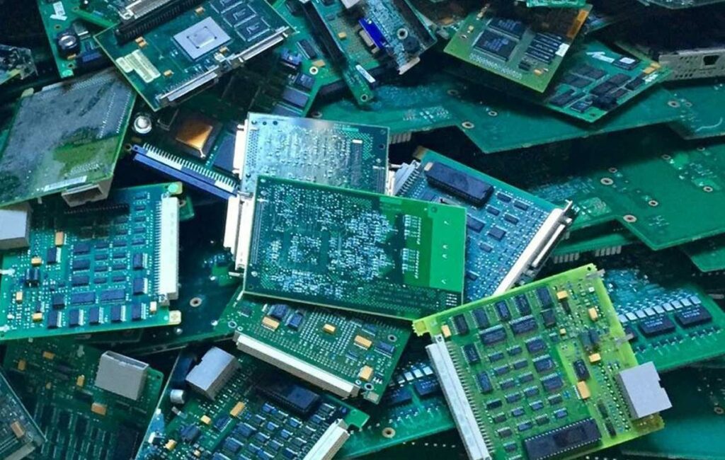
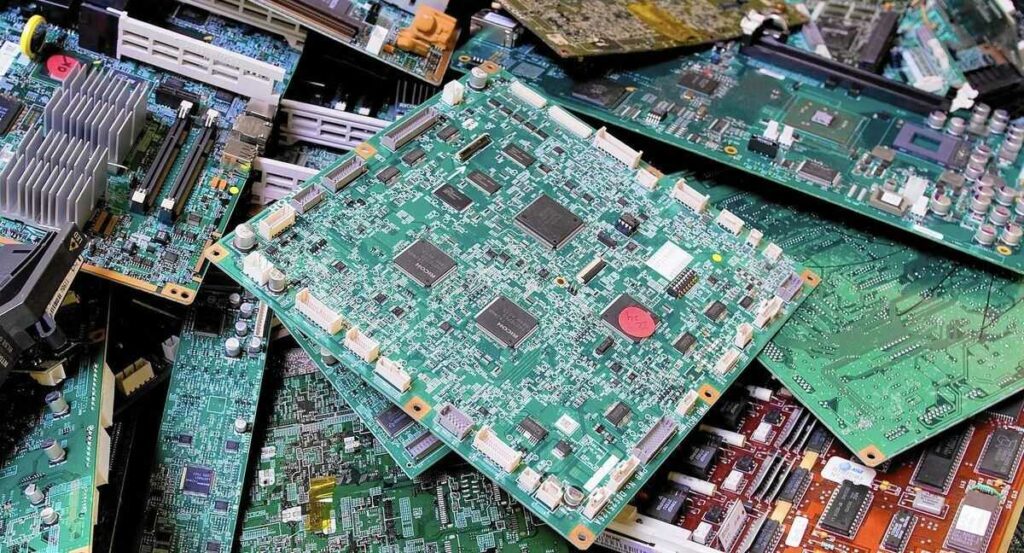
So in aggregate, while PCBs appear mundane at a glance, their material diversity mixes plastics, metals and other inorganics – making responsible separation essential to recycling viability.
Environmental & Economic Drivers for PCB Recycling
With complex material compositions and billions of units produced annually, electronic scrap PCB accumulation carries significant ecological and resource ramifications globally now acknowledged through policies like the European Union’s Waste Electrical and Electronic Equipment (WEEE), Restriction of Hazardous Substances (RoHS) and Registration, Evaluation and Authorization of Chemicals (REACH) directives alongside trade management reforms targeting dumping in developing nations.
Key factors compelling responsible PCB recycling practices include:
Toxicity – Lead, cadmium, beryllium, brominated flame retardants and other potentially hazardous materials used historically now face removal/substitution pressures but remain embedded in legacy or ongoing niche electronics. Unsound disposal contaminates soil/water posing health risks.
Scarcity – Deposits of economically minable rare earth metals and gold used in electronics get consumed far faster than their slow geological formation rates limit renewed discovery, making recovery via reuse the only renewable option.
Embedded Labor/Energy – The raw materials processing, specialized manufacturing equipment and global transport energy expended giving products their embodied technological value remains trapped unless reclaimed, arguing for additional lifecycles via responsible remanufacturing.
Policy Pressures – Stricter producer and retailer responsibility plus consumer right-to-repair government mandates coupled with disposal levies increasingly incentivize ecology-centered handling of retired or off-spec electronics including PCBs to minimize waste streams.
With associated stakes acknowledged, what strategies now enable economically upside and regulation compliant PCB reclamation?
PCB Recycling Process Overview
While seemingly daunting given complex buildups, closed-loop PCB recycling leveraging optimized disassembly automation followed by extraction of base materials and components using various physical, chemical and metallurgical separation techniques allow high yield harvesting for additional usage cycles minimizing net waste:
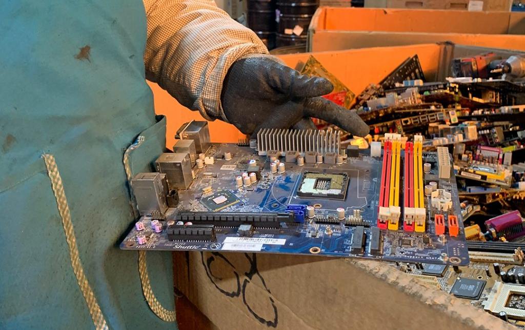
1. Collection & Sorting – Defunct boards get aggregated and triaged based on processing compatibility factors like age, technology generations, hazardous material content, etc.
2. Disassembly & Size Reduction – Machines strip usable sub-assemblies, components and larger metallic pieces while shredders break down scrap boards into 25mm fragments on average optimizing material liberation and transport efficiency.
3. Mechanical Processing – Hammer mills, grinding, screening, density separation, froth floatation and magnetic concentration progressively filter particulates into ferrous metals, non-ferrous metals, fiberglass and residue fractions ready for refining. Up to 95% purity gets achieved.
4. Chemical/Thermal Processing – Pyrolysis, leaching or solvent extraction apply heat, acids, gases and fluids using precision chemistry to isolate ultrafine metallic particulates of specialized elements like gold, platinum group metals and rare earth compounds present in small concentrations but carrying high inherent value.
5. Refining & Reuse – Final smelting, alloying and processing reconstitutes extracted materials like copper and tin into certified batches resupplied for manufacturing lines while precious metals get refined to 99%+ purity bullion ingots ready for global commodity markets driving circular economics. Recovered components also reenter appropriate supply chains when rated functional.
In addition to dedicated large scale e-waste recycling plants purpose built to leverage such methodical fragmentation, separation and reconstitution processes in country or abroad, a vibrant emerging ecosystem of smaller firms focuses upon maximum manual disassembly preservation targeting component reuse markets when boards get retired still working from IT equipment upgrades or commercial operation wind downs.
Printed Circuit Board Recycling Yield Rates
Across combined automated shred plus manual disassembly PCB recycling operations, materials recovery rates typically average:
- 35% Metals extraction for copper smelting
- 15% Useable component and subassembly harvest
- 30% Non-metallic material losses
So approximately half the embodied resource weight recirculates for additional usage cycles while losses still require capture improvements going forward through process refinements. However this outpaces by nearly 20X reclamation seen across plastics recycling generally for instance.
Key Challenges Around Recycling Printed Circuit Boards
For all the ecological and economic promise practices offer though, PCB recycling scaling globally faces headwinds including:
Identification Difficulties – Absence of naming standards, changing supplier codes and lack of historical databases impedes quickly validating board chemistry makeup for handling equipment. Improved labeling regulation helps address this upstream.
Separation Technology Gaps – No fully clean fractional decomposition exists for some composite blends like fiber-reinforced laminates or epoxy glues, limiting material purity recoveries as separation sciences still develop further solutions.
Low Cost Virgin Alternatives – Raw metal and petrochemical feedstock supplies lagging behind still growing electronic goods demand allows freshly mined or synthesized materials to undermine recycled pricing competitiveness until supply corrections occur.
Inconsistent Policy Enforcement – While tightening, e-waste regulations remain fragmented across global jurisdictions and often poorly enforced at local levels allowing unaccounted flows into gray recovery operations with lax standards, undercutting certified reprocessors.
User Apathy & Access Barriers – Despite swelling landfill volumes, most consumers remain unaware of recycling options or lack incentives to take action while companies worry about proprietary data risks when relinquishing old systems. More chain of custody clarity and compliance incentives help overcome reluctance hurdles.
Thankfully expansion of state mandated electronics take-back programs, growth in salvaged component distributors and a widening network of qualified sustainable IT asset disposition facilities and PCB recyclers make engagement increasingly turnkey over time even if hurdles persist in fully closing loops.
Outlook for Next Generation Printed Circuit Board Recycling
While current conventions already reclaim huge value from retired electronics, next generation printed circuit boards may further improve viability using principals of design-for-recycling and circular material flows to achieve near 100% regeneration:
Standardization & Modularity – Shared interoperability specifications allow swapping more components between board models while self-contained modular assemblies enable easier changeouts.
** Identification & Tracking** – IoT tagged boards tapping automatic sortation guide handling while embedded sensors monitor unit health to optimize service timing.
** Homerun Traces** – Conductive paths route through fewer layers with accessible discrete anchor points enabling simpler decoupling when reclaiming metals.
** Alternative Substrates** – Biopolymers like fungus mycelium have potential to replace thermoset composites if recycle-friendly thermoplastics still lack required electrical or mechanical attributes at scale.
So by beginning to envision printed circuit boards as temporary vessels circulating ingredients rather than fixed disposable commodities, product architects and policy framers may close loops further – where responsibility gets shared across the entire manufacturing, consumption and regeneration system.
Examples of Innovators Advancing PCB Recycling
Many companies worldwide at various scales now drive innovation advancing economically and ecologically balanced PCB recycling across the ecosystem:
Umicore – Multinational materials technology enterprise directing R&D into separation and refinement processes from battery metals to rare earth PGM recovery at industrial scale.
SIMS Recycling – Global leader in automated asset recovery disassembly technology coupled to certified responsible material reutilization networks.
Sea Serpent – Startup launching next generation aqueous plastic separation schemes to address fiberglass reinforced composites at origins.
Circular Computing – Cloud services provider incentivizing repaired data center server equipment reuse in emerging markets by paying for functional retrievals.
Restart Project – Non-profit network of community events and partnerships empowering grassroots repair, refurbishment and responsible e-waste handling.
So from basement tinkerers demonstrating repair viability to activists petitioning for better product stewardship laws all the way up to scientists perfecting digestion chemistry at massive smelters, an expanding landscape of entities coalesce worldwide to uplift PCB recycling.
Conclusion
In closing, establishing robust, economically self-sustaining printed circuit board recycling pathways requires awareness, accountability and advancement across makers, managers and users at all levels to generate circular flows minimizing electronic waste impacts.
With so many valuable and ecologically precarious materials concentrated in retired PCBs, embracing recyclability through improved design and diligent regeneration efforts continues growing in importance as more pivotal technology gets embedded across societies.
But by collectively addressing associated obstacles around economics, policy, technology and transparency – combined technical and social progress points towards electronics resource ecology becoming a regenerative system.
Frequently Asked Questions
Q: Can hobbyists safely recycle household small electronics themselves?
A: Generally not recommended as many compounds prove hazardous if crushed, heated or handled incorrectly. Utilize authorized municipal e-waste programs to enable responsible treatment. But building repair skills for reusing equipment remains great.
Q: Are any single critical raw materials found on PCBs today?
A: Advancements replace some niche materials like cobalt or tantalum. But sustained tech growth still depends on more common copper and rare earth elements in vast volumes with constraints needing improved circular access.
Q: How are economics balanced if mining new metals proves cheaper presently?
A: Pure cost analysis ignores externalities like pollution and health impacts that regulations force internalization of eventually. And finite deposits assure recycling will compete long term while promoting local jobs.
Q: Can meticulous manual disassembly enable high rates of PCB components reuse?
A: Absolutely – dedicated separation of functioning subsystems for resale preserves massive inherent value. But care must be taken handling older technologies possibly containing restricted hazardous materials requiring processing responsibility.
Q: Do any global certification programs help identify electronics recyclers following best practices?
A: Yes, respected auditing groups like R2 and e-Stewards certify firms across the IT asset disposition and electronics recycling industry meeting standards for transparency, environmental safety and social accountability. Searching for those designations signifies trustworthy partners.


