Printed circuit boards (PCBs) are essential components of virtually all modern electronics. From computers and smartphones to industrial controls and medical devices, PCBs provide the foundation for electronic circuits. But PCBs have not always existed in their current form. The origins of PCBs lie in their predecessor, the printed wiring board (PWB).
Understanding the distinction between PWBs and PCBs provides insight into the evolution of electronics manufacturing. While the terms are sometimes used interchangeably, there are important differences between printed wiring boards and printed circuit boards.
What is a Printed Wiring Board?
A printed wiring board (PWB) refers to an electrical board used to mechanically support and electrically connect electronic components using conductive pathways etched from copper sheets laminated onto a non-conductive substrate. PWBs were first developed in the 1940s as a solution to wire harness assembly difficulties experienced in complex electronic systems.
Key Characteristics of PWBs
- Non-conductive substrate made of phenolic resin or fiberglass laminate
- Copper foil etched to form conductive traces and connection pads
- Components inserted into holes drilled through board and soldered to traces
- Singe or double-sided variations; multi-layer boards later developed
- Industry standards instituted for dimensions and lead spacing
Printed wiring boards offered many advantages over traditional point-to-point wiring and breadboards:
- Greatly reduced assembly time and cost
- Improved reliability and performance
- Allowed automation of production processes
- Facilitated circuit design changes
- Supported miniaturization of electronic packages
PWBs drove major advancements in electronics manufacturing as they evolved from simple single-sided boards to complex multilayer boards between 1947 and 1965. However, they also had some limitations related to component connections that PCB technology later solved.
Transition from PWBs to PCBs
Printed circuit boards (PCBs) evolved from printed wiring boards as a means to overcome some of the interconnection challenges of PWBs. PCBs began emerging in the 1950s as engineers experimented with incorporating conductor patterns on both sides of boards and plating-through holes to form connections between layers.
Several key developments facilitated the transition from PWBs to PCBs:
- Etching processes – Improved etching techniques allowed finer features on both sides of boards. This enabled double-sided PWBs and then multilayer PCBs.
- Plated-through holes – Electroplating the walls of drilled holes electrically connected both sides of boards and multiple layers in multilayer PCBs.
- Solder masks – Solder masks limited solder spreading and reduced short circuits on crowded boards.
- Component packaging – Smaller discrete components like transistors and DIPs allowed higher circuit densities.
- CAD tools – Computer-aided PCB design automated board layout.
By the late 1960s, PCBs offering greater miniaturization, component density, and assembly efficiency had largely replaced PWBs.
Comparison of PWBs vs PCBs
While similar in many ways, PWBs and PCBs have some distinct differences:
| Parameter | Printed Wiring Boards | Printed Circuit Boards |
|---|---|---|
| Conductive Traces | Single-sided or double-sided | Multilayer common |
| Holes | Component leads inserted and soldered | Plated-through holes connect layers |
| Components | Discrete wires, tubes, transistors | Surface-mount and integrated circuit packages |
| Circuit Density | Limited due to component sizes | High density with smaller components |
| Design | Manual layouts | CAD software automated design |
| Materials | Phenolic or epoxy laminates | FR-4, polyimide, ceramics, composites |
| Processes | Etching and drilling | Improved photolithography and plating |
| Applications | Early radio, TV, and computer | All modern electronics |
Some key differences that highlight PCB advancements:
- Multilayer boards – Allow increased component density and complex circuitry
- Plated through holes – Enable connections between layers and doublesided mounting
- Solder masks – Improve board yields and circuit isolation
- Component types – Higher densities possible with microelectronics packages
- Automated design – Essential for complex PCB layouts and routing
- Advanced materials – Facilitate miniaturization and performance increases
So while PWBs initiated the printed board industry, PCBs accelerated electronics innovations through their enhanced capabilities.
PWB Construction and Materials
Printed wiring boards provided the foundation for PCB advancement. Early PWB fabrication involved laminating copper foil onto phenolic resin composites. The copper traces were manually etched and components inserted into drilled holes.
PWB Substrate Materials
The earliest PWB materials were phenolic resin composites like paper or linen reinforced phenolic. These were eventually supplanted by epoxy resin composites, including:
- Paper epoxy – Paper fabric reinforced epoxy resin
- Cotton epoxy – Woven cotton cloth reinforced epoxy
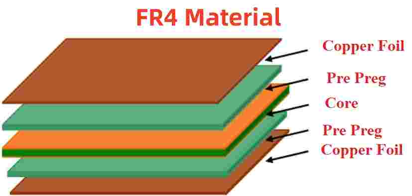
- Glass epoxy (FR-4) – Woven fiberglass cloth reinforced epoxy
Epoxy provided better mechanical and electrical properties than phenolic resins. FR-4 glass epoxy became the dominant PWB substrate material and was later adopted for PCB fabrication.
Copper Foil
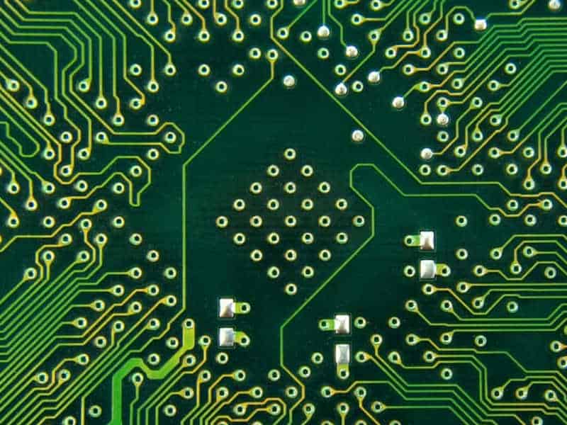
Copper foil provides the conductive traces in PWBs and PCBs. Rolled copper of 1⁄2 to 1 oz thickness was typically used, bonded to substrates with adhesive. Heavier foils permitted higher current capacity traces.
PWB Fabrication
The basic steps in PWB fabrication included:
- Cut layers of copper clad substrate to size
- Manually mask areas of copper to remain
- Chemically etch to remove unmasked copper
- Drill component holes
- Deburr holes
- Assemble components on board
- Solder component terminations
Multilayer PWBs were also produced by laminating etched double-sided boards together under heat and pressure. Holes were then drilled through the stack.
Evolution of PCBs
PCBs evolved from PWBs through innovations in materials, design, and fabrication processes:
Substrate Materials
Besides the FR-4 glass epoxy used in PWBs, PCBs adopted a range of dielectric substrate materials:
- CEM-1 to CEM-5 – Woven fiberglass reinforced epoxy
- Polyimide – Flexible, high temperature film
- PTFE – Low dielectric constant film for high frequencies
- Cyanate ester – High frequency, low loss resin system
- Ceramics – Alumina, aluminum nitride, boron nitride
Advanced materials enabled thinner substrates, microminiaturized traces, and improved electrical performance.
Laminates and Prepregs
Coated copper foil laminates and epoxy resin impregnated glass fabrics called prepregs are used to bond multilayer PCBs. Prepregs flow during lamination to fill spaces and bond layers into an integrated structure.
Conductors
Copper remains the primary conductor in PCBs due to its excellent conductivity and manufacturability. Some applications utilize gold, silver, or nickel plating.
Plated-Through Holes
A key PCB innovation, plated-through holes (PTHs) enable connections between layers in multilayer boards and double-sided component loading. PTHs are metallized with electroless and electrolytic copper and solder.
Solder Mask
The epoxy solder mask coating on PCBs limits solder spreading and prevents short circuits. This allows higher component densities.
Silk Screen
Like solder mask, the silk screen epoxy ink layer provides marking of component locations, polarities, and other identifiers without shorting traces.
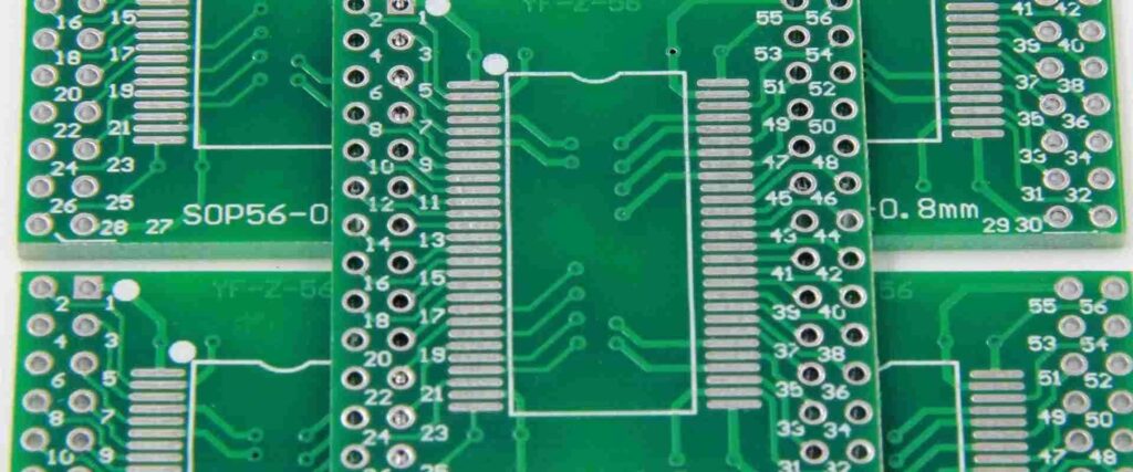
PCB Fabrication
Printed circuit boards are fabricated using an array of processes adapted from PWB production methods:
Substrate Preparation
Glasses fabrics, prepregs, and metal cores are laminated into multilayer boards under high heat and pressure before microetching.
Photolithography
A photosensitive dry film is applied to the PCB substrate. Ultraviolet light is used to transfer the conductor pattern from phototools to the photoresist.
Etching
Etching removes unwanted copper not protected by photoresist to form the conductive traces and pads. Common etchants include ferric chloride and ammonium persulfate.
Hole Drilling
High speed CNC mechanical drills or lasers drill thousands of tiny holes through the multilayer board for component leads and PTHs.
Plating
PTH walls are plated with copper using electroless plating to provide conductivity. Additional electroplated copper increases current capacity.
Solder Mask and Silkscreen
The solder mask and silkscreen coats are applied in the pattern specified by the design before final curing.
Surface Finishes
Coatings like immersion silver, immersion tin and organic solderability preservatives (OSPs) protect pads and traces from corrosion.
Final Assembly
Components are positioned and wave or reflow soldered to attach them to the board. Additional steps like conformal coating may also be used.
Automated assembly lines with robotic handling enable high volume PCB production.
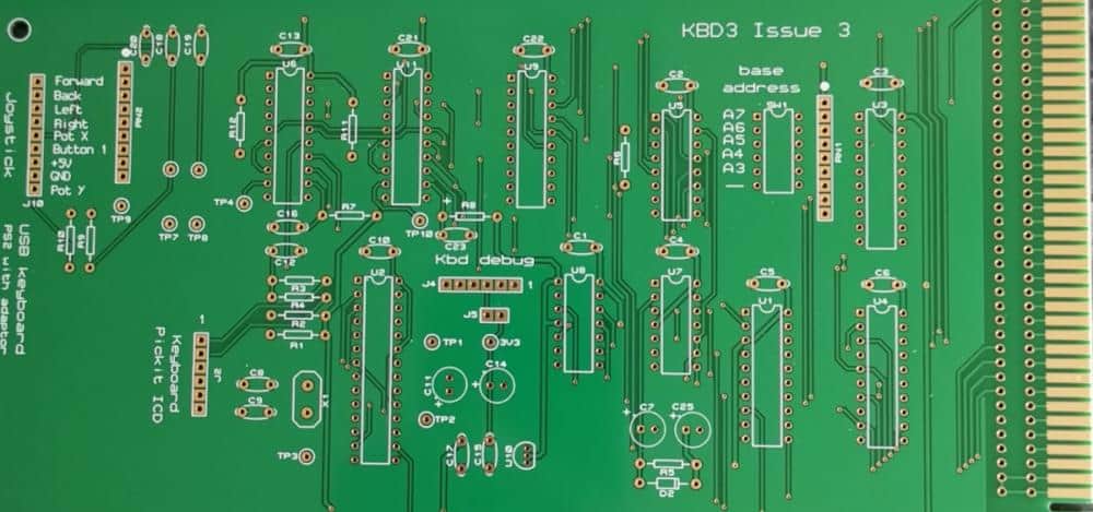
Applications of Printed Circuit Boards
Thanks to their capabilities, PCBs now form the backbone of nearly all electronic devices and systems. Major applications include:
Computers
Motherboards, expansion cards, graphic cards, storage media controllers and more rely on multilayer PCBs to interconnect components like microprocessors, memory, and peripherals.
Consumer Electronics
Phones, tablets, home appliances, smart devices, wearables, toys, and televisions depend on PCBs to perform their functions while meeting demands for miniaturization.
Automotive Electronics
Engine control modules, infotainment systems, GPS units, safety systems, lighting, and electric vehicle components all utilize carefully engineered PCBs for automotive performance.
Aerospace and Defense
Avionics controls, communications, targeting systems, and sensors for missiles, spacecraft, and aircraft feature specialized PCBs with tight tolerances.
Medical Devices
Hearing aids, imaging systems, diagnostics, prosthetics, and patient monitoring devices leverage complex multilayer PCBs to enable portability, precision, and functionality.
Industrial Electronics
Programmable automation controllers, motor drives, robotics, clean power, and process controls use PCB interconnects capable of high temperatures and vibration.
The Importance of Quality
Given the critical functions printed circuit boards enable in everything from cars to pacemakers, quality is paramount. Rigorous testing and process controls at every fabrication step ensure high reliability and performance.
PCB quality also requires continuous improvement and attention to details like:
- Material quality – Consistency and cleanliness
- Precision machining – Tight tolerances on traces and holes
- Contamination control – Cleanrooms, packaging, handling
- Comprehensive inspection – Automated optical, x-ray, electrical
- Qualified assemblers – Proper component placement and soldering
- QA documentation – Full traceability for defect prevention
By ensuring excellence throughout fabrication, even the most advanced PCB technologies reliably support our electronics-driven world.
Future Innovations
Printed circuit board technology continues advancing in step with electronics innovations. Expected PCB improvements include:
- Ultra-high density interconnects enabling increased functionality
- Built-in heat sinks and thermal management features
- Embedded actives like capacitors and resistors within the board
- Miniaturized microvias and laser drilled holes
- Flexible and stretchable boards for wearable devices
- Improved simulation, modeling, and design tools
- Sustainable, recyclable materials
Just as PCBs built upon the fundamentals of PWBs, ongoing enhancements in materials, design, and manufacturing will carry PCB technology far into the electronics future. The spirit of PCB innovation begun decades ago persists as engineers continue pushing the boundaries.
FQA
What was the first material used in printed wiring boards?
Phenolic resin composites were the first substrate materials used in PWBs, later displaced by epoxy resin materials like FR-4.
How did printed circuit boards improve upon printed wiring boards?
PCBs offered multilayer boards, plated through holes, smaller components, automated design, and advanced fabrication processes compared to PWBs. This increased density, performance, and reliability.
What are some key materials used in modern PCBs besides FR-4?
Some widely used PCB substrate materials include polyimide, PTFE, cyanate ester, and ceramics like aluminum oxide and aluminum nitride, along with laminates and prepregs.
What are some of the processes used to fabricate multilayer PCBs?
Primary PCB fabrication processes include imaging, photolithography, drilling, plating, etching, bonding, lamination, masking, and finishing like surface plating.
What demanding applications take advantage of multilayer PCB technology?
Cutting-edge applications for complex multilayer PCBs include consumer electronics, telecom networks, aerospace, medical devices, high-end computing, automotive, and industrial robotics.


