Introduction
PCB milling, also known as mechanical milling or routing, is the process of using a specialized milling machine to physically carve the traces and pads of a printed circuit board (PCB) from a block of substrate material. This allows hobbyists and engineers to rapidly prototype single or small batches of PCBs without the need for chemical etching or board fabrication from a PCB manufacturer.
PCB milling has become an accessible and affordable option for PCB prototyping thanks to the development of desktop CNC mills and milling software. Hobbyist mills can be purchased for a few hundred dollars, while more advanced mills with features like auto tool changing and drill heads can cost a few thousand dollars. When combined with CAD and CAM software to convert PCB designs into toolpaths, even beginners can machine their own PCBs with relative ease.
Advantages of PCB Milling
Here are some of the main benefits of using PCB milling for prototype PCB fabrication:
- Fast turnaround: PCB milling is extremely quick. Simple boards can be milled in under an hour, while more complex multi-layer boards may take a few hours. This compares favorably to the days or weeks it can take to order boards from a PCB fab.
- Low startup costs: Desktop PCB mills can be purchased for $200-$2000. No harsh chemicals are required like with etching. This makes PCB milling accessible to hobbyists and startups.
- Ideal for rapid prototyping: Milling is well suited to iteratively testing new revisions of a PCB design. Changes can be implemented quickly without needing to order full fabrication runs.
- Various substrate options: Milling works with FR-1, FR-4, Rogers, aluminum, and other substrates. No need to be limited to the materials offered by PCB fabs.
- Easy integration with CAD software: Most mills work seamlessly with PCB design software like Eagle, KiCad, Altium etc. The CAM file is generated with a few clicks.
Limitations of PCB Milling
While PCB milling has its benefits, it also has some limitations to be aware of:
- Lower precision: Milled traces are limited to 8-10 mil widths and spacings. Etching can achieve much finer trace resolution.
- Single-sided boards only: Milling can only carve one side of a board at a time. Multi-layer boards are not possible.
- Limited board sizes: Desktop mills max out around 12″ x 12″. Larger boards may require industrial mills.
- Slower than mass production: Each PCB must be milled individually. Large production runs are better suited to standard fabrication.
- Exposed traces/pads: The milling process leaves traces and pads exposed to the elements. Plating or soldermask/silkscreen is not applied.
- No vias: Since milling can’t drill holes, vias and through-hole components are not possible. Only surface mount parts may be used.
The PCB Milling Process
Here are the typical steps involved in the PCB milling process:
1. Design the PCB layout
- Create the circuit schematic and PCB layout in EDA software like Eagle, KiCad, Altium etc.
- Make sure to follow fabrication capabilities and design rules for milling:
- Minimum trace/space: 8-10 mils
- 1 oz copper thickness
- Clearance for drill bits around pads
- Finish routing, place components, add silkscreen layer etc.
2. Generate CAM file
- Open the PCB layout in the CAM software that came with the mill. Common options:
- FlatCAM (open source)
- Fritzing (open source)
- Carbide Copper (Carbide 3D)
- Fusion 360 (Autodesk)
- Select tool diameters, trace passes, drill sizes etc.
- Generate the toolpaths, gcode file, or other file for the mill.
3. Prepare the milling machine
- Mount the PCB substrate material to the bed – usually FR-1, FR-4, or Rogers. Vacuum hold-down is common.
- Install the appropriate end mill cutter bit into the machine spindle.
- Zero/reference the mill bit to the work coordinate system.
- Apply sacrificial material around the PCB if needed to prevent over-milling.
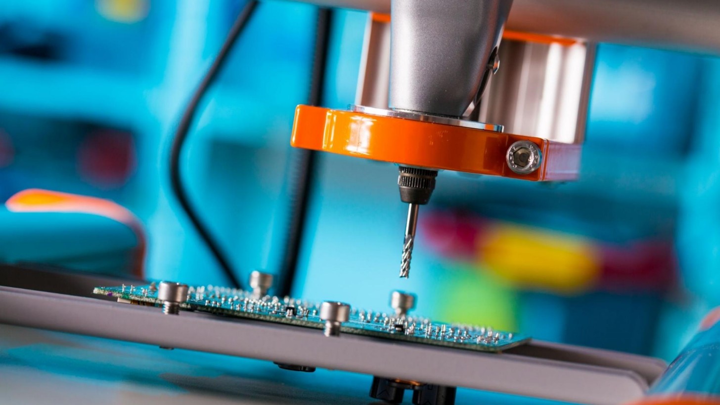
4. Perform the milling process
- Load the CAM gcode file into the milling machine.
- Run the program to first face-mill the top surface flat and smooth.
- The tool will trace out the PCB features in multiple passes at incremental depths, carving away substrate material until the traces and pads are isolated at the desired depth.
- Change bits as needed – a smaller end mill is often used for finer traces.
- For drilling holes, replace the end mill with a drill bit in the spindle.
5. Finish the board
- Carefully remove the finished PCB from the machine bed.
- Clean away debris and sacrificial material using compressed air, brushes, or isopropyl alcohol.
- Inspect for defects under a magnifier. Redo milling if needed.
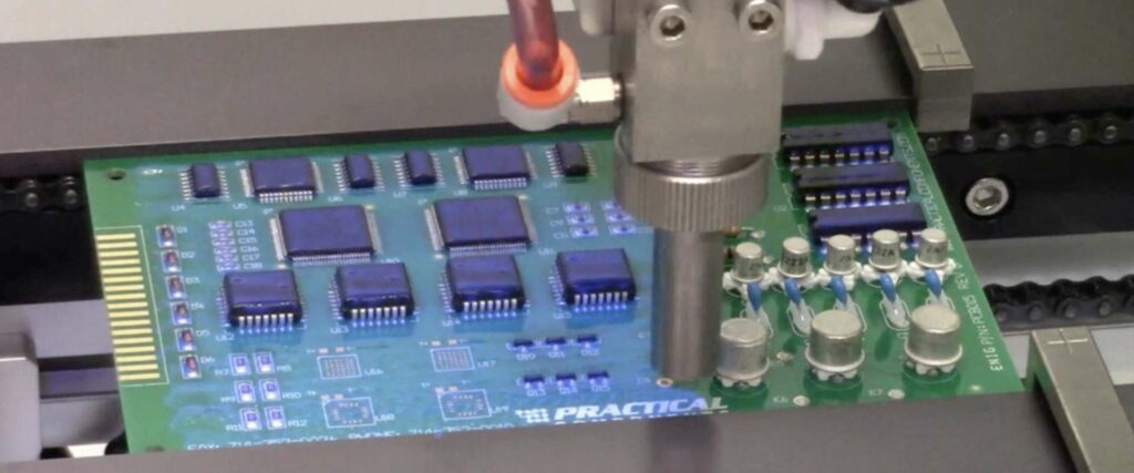
- Install components by soldering directly to the milled pads.
And that covers the basic workflow for prototyping a custom PCB using a desktop milling machine! With some practice, PCB milling allows rapid design iterations and lets you produce boards exactly how you want them.
PCB Milling Machines
There are a wide variety of desktop PCB milling machines available to suit different needs and budgets. Here are some of the most common options:
Entry-Level/Hobbyist Mills
- Bantam Tools Desktop PCB Milling Machine – Compact CNC mill starting at $3,199. Easy to use with integrated CAM software. ~10 mil resolution.
- OtherMill Pro – Low cost at $2,150. 10 mil traces, small footprint. Open source software.
- CNC 3020/3040 Routers – Generic mini-mills can be adapted for PCB milling. Require more user assembly and configuration. Cost $200-$500.
- PocketNC V2 – 5″ x 5″ milling area, 10 mil resolution. Very compact. Integrated touchscreen interface. $2,500.
High-End/Industrial Mills
- LPKF ProtoMat S104 – Considered the industry standard PCB prototyping system. 10 mil traces, auto tool change, drill head, large work area. ~$18,000.
- Bungard CCD – Powerful mills designed for high-end PCB work. Top of the line at over $30k. Auto tool change, precision spindle, vacuum bed.
- Other high-end makers – CAMTech, Insulectro, Vision, AccurateCNC, Minitech, APCB, MicroProtoSystems etc. Prices range from $10k-$50k.
The optimal mill depends on factors like work area size, desired feature size, tool change needs, material options, and budget. Desktop hobbyist mills offer an affordable introduction, while industrial machines provide premium performance.
PCB Milling vs Other Prototyping Methods
There are a few other common ways to prototype printed circuit boards in addition to milling. Here is how milling compares:
PCB Milling vs Etching:
- Milling is faster, easier, and lower cost than chemical etching. No hazardous chemicals to deal with.
- Etching achieves finer trace resolution down to 6 mils vs 8-10 mils for milling.
- Milling can create irregular board shapes more easily.
PCB Milling vs SLA 3D Printing:
- 3D printing achieves higher precision but is much slower and has higher material costs.
- Milling supports larger board sizes up to ~12″ x 12″. 3D printing has limited build volumes.
- 3D printing is best for very low volume with unique designs. Milling is better for prototyping small batches.
PCB Milling vs Ordering from a PCB Fab:
- Milling is much faster for prototyping – no need to wait days/weeks for fabrication.
- PCB fabs offer mass production, soldermask, silkscreen, vias, etc. Milling is limited to simple bare boards.
- Milling has low NRE costs. Fabs require minimum order quantities which can be expensive.
So in summary, PCB milling hits a sweet spot between DIY etching and 3D printing for quick, low-cost functional prototyping. It enables iterative testing not possible when ordering from a professional PCB manufacturer.
Tips for Successful PCB Milling
Here are some tips for getting the best results when milling your own PCBs:
- Use the right substrate material. FR-1 and FR-4 are common. Rogers materials offer higher performance for RF boards.
- Generate multiple toolpaths/passes for finer details and smoother milling. In CAM software increase passes for smaller end mills.
- Apply sacrificial material around the board edges to prevent over-milling. Blue painter’s tape works well.
- Use compressed air and a brush to thoroughly clean boards after milling to remove debris before soldering.
- Work in small increments when dialing in milling depth, speeds, feeds etc. Test on cheap scrap material first.
- Replace dull end mills for cleanest cuts. Carbide cutters offer longevity over cheaper high-speed steel.
- Use a thinner end mill for the final pass to achieve the smallest trace spacing possible.
- Minimize board warpage by securing substrate firmly to spoilboard. Vacuum hold-downs produce best results.
- Add fiducial markers to the board edges to assist with component placement after milling.
With practice, you’ll be able to consistently mill professional-quality PCB prototypes. Paying attention to details like workholding, tooling condition, and cleanliness helps achieve great results.
Applications of PCB Milling
Some examples of where PCB milling is commonly used:
- Prototyping – Test new PCB designs before investing in full production board fabrication. Allows rapid design revisions.
- Low-volume production – For projects only needing a small number of boards, milling avoids high prototyping costs.
- Education – Milling provides hands-on experience working with PCBs in academic lab settings.
- Custom/novel materials – Milling enables use of exotic substrate materials that regular PCB fabs don’t offer.
- RF/microwave boards – Milling Rogers and other high-frequency boards that require tight impedance control and tolerance.
- Repairing boards – Small milling machines can modify existing boards by re-routing connections.
- Making one-off interface boards – Quickly mill a board to interface sensors, motors, or other components to a system.
- Artistic/decorative pieces – With careful fixturing, mill intricate PCB-based objects, art, jewelry, nameplates, etc.
PCB milling eliminates the turnaround time associated with board fabrication, empowering inventors and engineers to rapidly test their designs built with their own hands.
Conclusion
PCB milling is an accessible and flexible prototyping solution for hobbyists and professionals alike. The ability to quickly go from a circuit design to a physical PCB enables rapid design iteration and hands-on learning.
While milling has limitations on feature size, layer count, and scale of production compared to commercial board fabrication, it fills an important niche. The low cost machines, open source software, and straightforward process lets innovators build prototypes on their own schedules, supporting creativity and experimentation.
With practice, it’s possible to mill professional-quality PCBs with fine features that can be populated with components. Milling won’t fully replace traditional PCB fabrication, but will continue empowering agile prototyping and design exploration.
Frequently Asked Questions
What materials can be milled?
The most common materials are FR-1 and FR-4 fiberglass. Rogers PCB materials are also commonly milled for high-frequency RF applications. Other options include ceramics, aluminum, Woods metal, and plastics like HDPE, though they are less commonly used.
What accuracy/precision can be achieved?
The best desktop mills can achieve about 8 mil trace/space resolution. Industrial mills are capable of 6 mil resolution or better. Precision is affected by many factors including machine rigidity, runout, tooling condition, and workholding.
How are through-hole components handled?
Milling can’t directly make vias or drill holes. Some options are to hand drill holes, use surface-mount components only, or make slotted holes that components can drop into. Soldering wires through milled slots is also an option.
How long does it take to mill a board?
Simple boards with large features can mill in under an hour. More complex boards with small trace sizes may take multiple hours. The milling time is highly dependent on the board design, size, and feed rates.
Can both sides of a PCB be milled?
Traditional milling can only directly work on one side of the board at a time. The board would need to be flipped and re-fixtured to mill the opposite side. Some advanced techniques use two synchronized spindles to mill both sides simultaneously.


