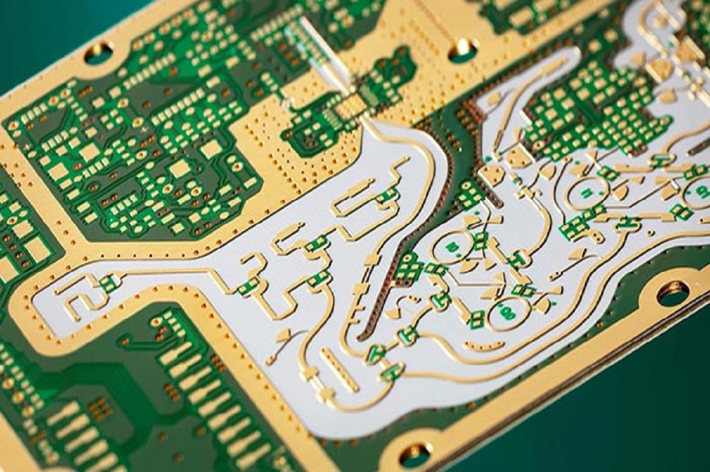
High frequency PCB design requires special layout considerations to ensure signal integrity and minimize electromagnetic interference (EMI). As operating frequencies increase into the MHz and GHz range, trace lengths become a significant fraction of the signal wavelength, and transmission line effects dominate. Proper impedance control, layer stacking, decoupling, and grounding are essential for robust high frequency performance. This article provides an overview of best practices for high frequency PCB layout.
High Frequency Effects
At high frequencies, traces exhibit transmission line behavior and must be treated as controlled impedance lines. Key effects to consider are:
- Reflections – Impedance discontinuities cause partial reflection of the signal. This can lead to ringing and noise.
- Cross-talk – AC coupling occurs between traces in close proximity, interfering with signal quality.
- Radiation – Unwanted EMI emissions radiate from traces and cause electromagnetic compliance (EMC) issues.
- Loss – Skin effect and dielectric losses become significant, attenuating signals.
To mitigate these effects, impedance control, shielding, and proper stackup design are essential.
Transmission Lines and Impedance Control
Every PCB trace behaves as a transmission line with characteristic impedance determined by its geometry and material properties:Copy code
Z0 = (L/C)^0.5 L = inductance per unit length C = capacitance per unit length
For a microstrip trace over a reference plane, a simple approximate formula is:Copy code
Z0 = (87/√εr + 1.41) * ln[(5.98*h) / (0.8*w + t)] εr = dielectric constant h = trace height above plane w = trace width t = trace thickness
To prevent reflections, traces must be routed with controlled impedance matched to their source and load terminations. Common values are 50Ω or 75Ω. Key techniques include:
Impedance Control Techniques
- Use impedance calculators to determine trace widths and spacing for target Z0.
- Minimize impedance discontinuities at trace junctions using tapers, stubs, or matching networks.
- Use smooth bend radii (>3X trace width) to minimize abrupt impedance changes.
- Avoid 90° corners. Use 45° chamfers or arc shapes instead.
- Minimize length of uncontrolled impedance stubs.
Layer Stackup
A well-designed layer stackup is crucial for impedance control, EMI management, and signal quality. Guidelines include:
- Place critical signals on internal layers next to reference planes for shielding.
- Use thick reference planes (>2x layer thickness) for low impedance.
- Separate analog and digital domains on different layers.
- Provide uninterrupted ground return paths under traces. Avoid plane cuts and gaps.
- Use stripline (signal-plane-signal) for differential pairs. Controlled impedance depends on plane spacing.
- Ensure dielectric thickness and εr allow target Z0 for microstrip and stripline traces.
Bypass Capacitors
Decoupling capacitors provide charge reservoirs to stabilize supply voltages during fast transient loads. Each IC power pin should have an adjacent bypass cap. Additional guidelines:
- Use a mix of values for broad frequency decoupling (0.1uF, 0.01uF etc).
- Choose low ESR, X7R, or NP0 ceramic caps. Avoid piezo and electrolytic types.
- Place caps immediately next to ICs with minimal trace length to Vdd/Gnd.
- Provide both shunt and serial decoupling for aggressive transient loads.
- Supplement with bulk tantalum or polymer caps at PCB input supply.
Signal Integrity
Cross-talk and reflections can cause signal quality issues. Recommendations to ensure signal integrity:
- Use ground guard traces or ground planes between critical signals.
- Route aggressive signals first, then route sensitive nets.
- Minimize parallel trace length and avoid 90° trace intersections.
- Use differential signaling where possible. This inherently cancels cross-talk and noise pickup.
- Limit trace length mismatches in differential pairs to < 15 mils.
- Add series termination resistors at trace ends to damp reflections. Values match Z0.
- Use impedance matching networks at connectors or add ferrite beads to damp resonances.
Power Integrity
Robust power distribution prevents unwanted noise coupling into sensitive circuits. Guidelines include:
- Use large flood fills for Gnd and Vdd planes. Avoid islands.
- Provide multiple via contacts from surface traces to planes to reduce inductance.
- Separate analog and digital power using splits in the power planes.
- Filter supplies to sensitive analog areas using ferrite beads and bypassing.
- Where planes shift between layers, stitch with closely spaced vias.
EMI Control
It is crucial to prevent layouts from radiating excessive EMI throughout the spectrum. Recommendations include:
- Enclose sensitive or noisy areas in shielded compartments. Use many vias to connect compartments to bottom Gnd plane.
- Strategically place component shields, sheet metal, and wire mesh for additional localized shielding.
- Use a bandgap fill pattern (vias/polygons) in unused board areas to reduce EMI resonances.
- Avoid slots or large openings in ground planes. These will radiate emissions.
High Speed Routing Techniques
In addition to impedance control, high frequency traces require specific routing techniques for signal quality.
Matched Propagation Delays
Length matching ensures synchronized arrival times for critical signals like clocks or differential pairs. Guidelines:
- Match lengths to within 10-15 mils for traces with fast edge rates. Longer mismatches allowable for slower signals.
- Match electrical length including bends. Outer traces in bends have longer propagation paths.
- Serpentine outer traces to equalize delay with short inner traces.
- Use delay matching networks if perfect length matching is not possible.
Minimizing Reflections
Reflections occur at impedance discontinuities and open stubs. Techniques to minimize:
- Avoid open-ended traces. Route to terminate at matching impedance loads.
- Limit stubs to < λ/10. Use accordion routing to equilibrate stubs.
- Use circular back-drilling of unused vias to remove their open stub effects.
- Connect unused board connectors to termination networks or loads.
Cross-Talk Mitigation
Capacitive coupling creates cross-talk between parallel traces. Methods to reduce:
- Increase spacing between traces, at least > 3x dielectric thickness.
- Avoid routing >3 traces in parallel over long distances. Use ground traces as shields between signals.
- Route with perpendicular trace intersections instead of parallel runs.
- Use ground guard traces on at least one side of aggressor trace to shield victim lines.
Termination
Signals reflecting back and forth can cause overshoot and ringing. Termination suppresses reflections:
- Series terminate by adding resistor matching Z0 near load. Reduces reflections from receiver.
- Parallel terminate by adding shunt resistor to ground near source. Prevents reflections from the far end.
- Use RC networks for damped termination. Capacitor shunts AC to ground while resistor matches Z0.
- Formultidrop topologies, use AC termination at each drop to block reflection while passing DC.
Vias
Vias can introduce impedance discontinuities, crosstalk, and reflections:
- Minimize via transitions along controlled impedance traces.
- Stagger adjacent via barrels to increase spacing and reduce coupling.
- Back-drill unused segment of buried vias to remove their stub effects.
- Place ground vias adjacent to signal vias for return current continuity.
- Use filled thermal relief connections instead of spokes for lower inductance.
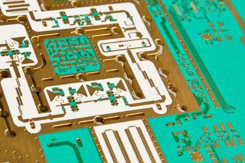
Example Stackup
Here is an example 6-layer high frequency PCB stackup with good SI, PI, and EMI characteristics:
Key features:
- Thick uninterrupted ground planes adjacent to all signals for controlled impedance and shielding.
- Ground/power plane separation to prevent coupling. Stitching vias bridge where planes shift.
- Analog and digital supplies separated. Digital section has more aggressive decoupling.
- Bandgap EMI fill pattern around the board perimeter ties planes together.
- No plane cuts under critical ICs. Continuous return paths provided.
- Stripline routing for clock nets immune to external noise.
Simulations
Validate layouts using EDA tools before manufacturing PCBs:
- Run signal integrity simulations to verify clean eye diagrams and waveforms.
- Perform power integrity analysis under various load conditions to ID noise issues.
- Model EMI performance with IBIS models and simulate radiated emissions.
- Thermal analysis to ensure components operate within temperature specs.
Adjust the layout as needed based on simulation results before final release.
Conclusion
High frequency PCB layout requires special attention to transmission lines, impedance control, layer stackup, bypassing, and signal routing techniques. When executed well, this enables designs that perform up to multi-GHz frequencies with acceptable signal quality, power integrity, thermal dissipation, and EMI. Simulation and analysis provide validation of the layout before manufacturing. With diligent engineering and adherence to sound principles, nearly any high frequency application can be accommodated with the PCB as a robust and repeatable signal foundation.
Frequently Asked Questions
What is the most important thing for high frequency PCB layout?
Controlling impedance is the most crucial task, as impedance mismatches lead to signal reflections and loss of integrity. Use impedance calculators to design traces for target Z0, minimize discontinuities, and implement controlled-impedance routing.
How low should I keep dielectric constants in the PCB stackup?
Lower dielectric constants allow wider lines for a given impedance, reducing losses. But with εr < 3, the stackup thickness becomes impractical. εr of 3-4 provides a good compromise. High performance materials up to εr ~10 can work with very thin dielectrics.
What is the effect of higher temperature on a PCB dielectric?
Increasing temperature reduces dielectric constant and increases loss tangent. Both factors tend to lower impedance slightly. This effect should be modeled to ensure impedance targets are still met at max operating temps.
How do I decide between microstrip, stripline or dual stripline routing?
Microstrip is easiest to implement but provides no shielding from EMI. Stripline gives superior noise immunity but requires vias or clearances for component mounting. Dual stripline is good compromise if the stackup allows the additional reference planes.
How often should power and ground planes be stitched together?
A good rule of thumb is to stitch planes together at intervals less than λ/20. For example, in a PCB with signals up to 5 GHz, stitching vias should be used at least every 1.5 cm. More frequently is even better for decoupling purposes.


