Introduction
In the ever-evolving world of electronics, the demand for compact and high-density packaging solutions has led to the development of advanced interconnect technologies. One such technology that has gained widespread adoption is the Ball Grid Array (BGA). BGA packages are surface-mount integrated circuit (IC) packages that employ an array of solder balls as the primary interconnection mechanism between the IC and the printed circuit board (PCB). This article delves into the intricacies of BGA technology, exploring its design, manufacturing processes, advantages, and applications.
What is a Ball Grid Array (BGA)?
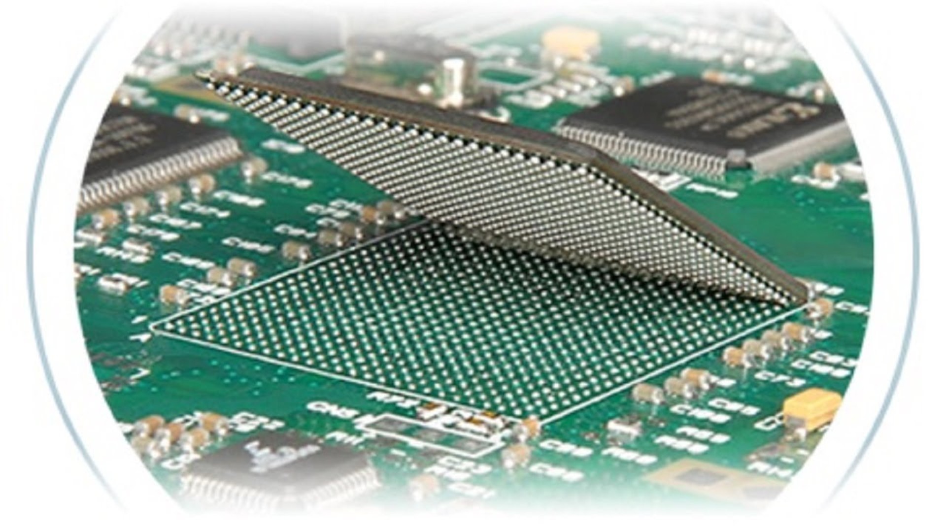
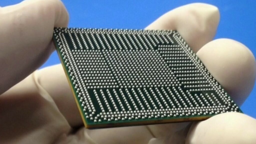
A Ball Grid Array (BGA) is a type of surface-mount package used for integrated circuits (ICs). It features an array of solder balls on the bottom surface of the package, which serves as the interconnection points between the IC and the PCB. These solder balls are arranged in a grid pattern, providing a high density of input/output (I/O) connections.
Key Components of a BGA Package
A typical BGA package consists of the following components:
- Integrated Circuit (IC): The semiconductor device or chip that performs the desired electronic functions.
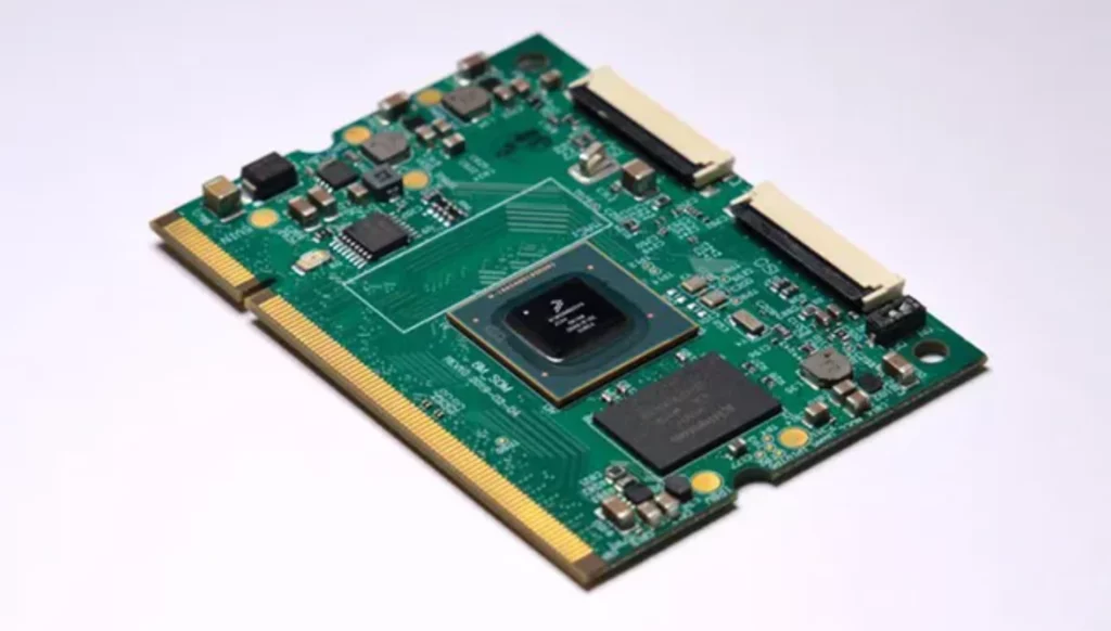
- Substrate: A multi-layer laminated structure that provides electrical connections between the IC and the solder balls.
- Solder Balls: Spherical solder balls attached to the bottom surface of the substrate, forming the array pattern.
- Underfill: A specialized epoxy resin dispensed between the IC and the substrate, providing mechanical support and stress relief.
- Overmold: A protective encapsulant material that covers the IC and portions of the substrate, providing mechanical protection and environmental shielding.
BGA Package Types
BGA packages can be categorized based on various factors, including the substrate type, package size, and ball pitch (the distance between adjacent solder balls). Some common BGA package types include:
- Plastic BGA (PBGA): These packages use a plastic substrate and are generally less expensive than ceramic BGAs.
- Ceramic BGA (CBGA): These packages employ a ceramic substrate, offering better thermal conductivity and higher reliability.
- Micro BGA (μBGA): These are smaller BGA packages with a ball pitch of 0.8 mm or less, suitable for space-constrained applications.
- Fine-Pitch BGA (FBGA): These packages have a ball pitch of 1 mm or less, enabling higher I/O densities.
- Super BGA (SBGA): These are high-performance BGA packages with advanced features like heat slugs or integrated heat spreaders.
BGA Manufacturing Process
The manufacturing of BGA packages involves several intricate processes, including:
- Wafer Fabrication: The IC is fabricated on a semiconductor wafer using various processes like deposition, lithography, and etching.
- Wafer Dicing: The wafer is diced into individual IC chips or dies.
- Die Attachment: The IC die is attached to the substrate using a specialized adhesive or solder.
- Wire Bonding or Flip Chip Bonding: Electrical connections are made between the IC and the substrate using either wire bonding or flip chip bonding techniques.
- Underfill Dispensing: A specialized epoxy resin is dispensed between the IC and the substrate to provide mechanical support and stress relief.
- Solder Ball Attachment: The solder balls are attached to the substrate using a solder ball placement or solder ball drop process.
- Overmolding: The IC and portions of the substrate are encapsulated with a protective overmold material.
- Singulation: The individual BGA packages are singulated from the panel or strip.
- Testing and Inspection: The BGA packages undergo various electrical and visual inspections to ensure quality and functionality.
Advantages of BGA Packages
BGA packages offer several advantages over other packaging technologies, including:
- High Density: BGAs can accommodate a large number of I/O connections in a compact footprint, enabling high-density and high-performance designs.
- Improved Electrical Performance: The shorter signal paths in BGAs result in reduced inductance and capacitance, improving electrical performance and signal integrity.
- Enhanced Thermal Dissipation: The array of solder balls provides an efficient thermal path for heat dissipation, making BGAs suitable for high-power applications.
- Surface Mount Compatibility: BGAs are designed for surface mount assembly, enabling efficient and cost-effective manufacturing processes.
- Improved Reliability: The sturdy mechanical design and underfill material in BGAs provide enhanced resistance to thermal and mechanical stresses.
Applications of BGA Packages
BGA packages are widely used in various electronic applications due to their advantages and capabilities. Some common applications include:
- Microprocessors and System-on-Chip (SoC) Devices: High-performance microprocessors and SoCs often employ BGA packaging to accommodate their high I/O counts and thermal dissipation requirements.
- Graphics Processing Units (GPUs): GPUs in computers, gaming consoles, and mobile devices commonly use BGA packages to handle the high data throughput and thermal loads.
- Networking and Communication Equipment: BGAs are extensively used in networking devices, routers, and communication equipment due to their high-density and performance capabilities.
- Mobile Devices: Smartphones, tablets, and other portable electronics leverage BGA packages for their compact size and high-density interconnections.
- Automotive Electronics: The reliability and ruggedness of BGA packages make them suitable for automotive applications, such as engine control units and infotainment systems.
- Industrial and Medical Equipment: High-performance BGAs are employed in industrial control systems, medical imaging devices, and other specialized equipment.
Challenges and Considerations
While BGA packages offer numerous advantages, they also present some challenges and considerations:
- Rework and Repair Difficulties: Due to the high-density interconnections and the presence of the overmold, reworking or repairing BGA packages can be challenging and may require specialized equipment and techniques.
- Thermal Management: Effective thermal management is crucial for BGA packages, especially in high-power applications, to prevent overheating and ensure reliable operation.
- Board-Level Reliability: The solder joint reliability between the BGA package and the PCB is a critical factor, influenced by factors such as thermal cycling, mechanical stresses, and substrate characteristics.
- Manufacturing Complexity: The manufacturing process for BGA packages is relatively complex and requires specialized equipment and expertise, which can increase production costs.
- X-Ray Inspection Limitations: Due to the high-density interconnections and the presence of the overmold, X-ray inspection of BGA packages can be challenging, making defect detection more difficult.
Future Trends and Developments
The demand for higher performance, increased miniaturization, and advanced functionality continues to drive the evolution of BGA technology. Some future trends and developments in BGA packaging include:
- Finer Pitch and Higher Density: The pursuit of even higher I/O densities and smaller package sizes is leading to the development of finer pitch BGAs with smaller solder ball diameters and tighter spacing.
- Advanced Substrates: The use of advanced substrate materials, such as low-loss dielectrics and embedded passive components, is enabling improved electrical performance and higher integration levels.
- 3D and Stacked Die Packaging: Stacking multiple dies or integrating different functionalities within a single BGA package is becoming more prevalent, enabling higher performance and functionality in compact form factors.
- Embedded Chip Packaging: Embedding the IC directly into the substrate or interposer, eliminating the need for an overmold, is an emerging trend that can improve thermal and electrical performance.
- Heterogeneous Integration: The integration of different semiconductor technologies, such as logic, memory, and sensors, within a single BGA package is enabling the development of highly integrated and multifunctional systems.
Frequently Asked Questions (FAQ)
- What is the difference between a BGA and a QFP (Quad Flat Package)? A: The main difference lies in the interconnection mechanism. BGA packages use an array of solder balls for interconnection, while QFP packages employ leads or pins arranged along the package edges.
- Can BGA packages be repaired or reworked? A: While it is possible to rework or repair BGA packages, the process is generally more challenging and complex compared to other package types due to the high-density interconnections and the presence of the overmold.
- What are the typical ball pitches used in BGA packages? A: Common ball pitches for BGA packages range from 1.27 mm (0.05 inches) down to 0.4 mm (0.016 inches) or even smaller for advanced packages. The pitch determines the I/O density and package size.
- How does the underfill material contribute to the reliability of BGA packages? A: The underfill material, typically an epoxy resin, provides mechanical support and stress relief between the IC and the substrate. It helps absorb thermal and mechanical stresses, improving the overall reliability and solder joint integrity of the package.
- What are some thermal management considerations for BGA packages? A: Effective thermal management is crucial for BGA packages, especially in high-power applications. Techniques such as heat slugs, integrated heat spreaders, and thermal vias can be employed to improve heat dissipation. Additionally, proper PCB design and thermal interface materials play a role in managing thermal loads.
By providing a comprehensive understanding of BGA technology, this article aims to equip readers with the knowledge necessary to appreciate the significance of this packaging solution in the ever-advancing world of electronics.


