Introduction
Printed circuit boards (PCBs) are at the heart of all electronic devices and equipment. Traditional PCB fabrication involves complex processes like etching, drilling and plating. An emerging technological innovation now enables 3D printing of functional multilayer PCBs cost effectively using modified desktop 3D printers and novel materials. This article explores this new 3D PCB printing technology, its benefits, applications and future outlook.
Overview of 3D Printed PCB Technology
3D printed PCBs refer to functional printed circuit boards with conductive traces embedded within 3D printed substrates. They are fabricated using regular desktop fused deposition modeling (FDM) 3D printers by combining polymer filament substrates with chemically treated conductive filaments.
This enables complete end-to-end 3D printing of electronic circuits within 3D models without any additional processing steps. Components can be directly assembled onto 3D printed PCBs using soldering or conductive adhesives.
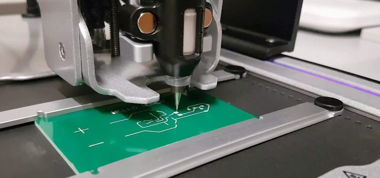
Researchers at Nanyang Technological University, Singapore demonstrated this possibility of 3D printing multilayer PCBs using a desktop 3D printer.
Image Credit: Nanyang Technological University
Conductive Filament Technology
The technology breakthrough enabling 3D printed PCBs is the conductive filament. It is a thermoplastic polymer material like polylactic acid (PLA) or acrylonitrile butadiene styrene (ABS) with embedded conductive particles like graphene or carbon nanotubes.
Graphene infused filaments exhibit sheet resistivity between 5-15 ohm/sq allowing printed tracks to be used as conductors. Copper fillings are also being explored in conductive filaments.
Working in conjunction with non-conductive substrate filament, it permits 3D printing of electronic circuit traces at micrometer resolution embedded within the 3D printed board structure.
Process of 3D Printing PCBs
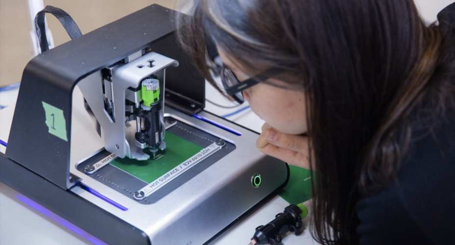
A regular desktop FDM 3D printer can be modified to print multilayer PCBs by using conductive filament for inner layer traces and non-conductive substrate for outer layers.
The typical process involves:
- Designing the PCB layout digitally using any electrical CAD software.
- Importing the PCB file into a 3D modeling software like SolidWorks and defining vertical layer structure.
- Slicing the 3D model file into layers and generating G-Code toolpath instructions for the 3D printer.
- Loading conductive graphene/carbon PLA filament when printing conductive traces and regular PLA for substrate layers.
- Printing the layers by extruding conductive and non-conductive filaments according to the toolpath.
- Automated switching of filament spools enables printing the complete multilayer 3D PCB in one production run.
- Conductive epoxy or solder paste can be used to mount SMD components on pads.
This video shows the complete process of designing and 3D printing a PCB using conductive filaments.
Benefits of 3D Printed PCB Technology
Faster Prototyping
The ability to directly 3D print working PCB prototypes on the desktop enables electronics designers to fabricate circuits much faster without any external processing.
Design Flexibility
Circuit layers can be conformally embedded within 3D prints allowing greater layout flexibility. Components integrate tightly within 3D mechanical structures.
Lower Costs
Eliminates the need for expensive PCB fabrication equipment like etching machines or plating lines. Raw materials are also low cost.
Simplified Process
No chemical processing like etching, plating, waste treatment needed. Design to finished board using a single 3D printer.
Compact Design
Enables dense, compact layout of circuitry integrated seamlessly within 3D printed enclosures and assemblies.
Customizability
Easy to customize PCB designs and rapidly iterate improvements. Small batches feasible.
Materials Used in 3D Printed PCBs
Some of the core materials used in the 3D printed PCB process include:
1. Conductive Filament
- PLA or ABS filament with graphene, carbon or copper fillers
- Provides sheet resistivity of 5-15 ohm/sqm for conductive traces
2. Substrate Filament
- Regular PLA or ABS forms non-conductive substrate layers for insulation
- Can be doped with ceramic/glass fillers to improve rigidity
3. Solder Paste
- Used to attach SMD components onto pads
- Eases component Assembly after 3D printing
4. Conductive Epoxy
- Alternate option to solder paste
- Bonds components and forms reliable connections
Applications of 3D Printed PCBs

Some potential applications that can benefit from the 3D printed PCB innovation:
1. Functional Prototyping
Rapidly printing PCB prototypes for form, function and fit evaluations during product development.
2. Low Volume Production
For niche products like customized electronics equipment, IoT sensors.
3. Education & Training
Enables STEM education exposing students to 3D printing and electronics.
4. Wearable Devices
Directly embedding printed circuits into wearable product enclosures like smart watches.
5. Printed Antennas
Fabricating 3D antennas and waveguides using conductive printable materials.
6. Printed Sensors
Embedding various printed sensors like temperature, pressure into 3D products.
7. Robotics
Printed flex circuits to interconnect moving parts and joints in robots.
8. 3D Electronics
Conformally 3D packaging electronic assemblies with embedded actives and passives.
Challenges With 3D Printed PCB Technology
While promising, certain limitations need to be addressed before wider adoption of 3D printed PCB technology:
1. Lower Conductivity
Printed traces have higher resistivity than copper traces, leading to losses at high frequencies.
2. Lower Resolution
Minimum achievable trace size is 100um compared to 5-10um using lithographic PCB etching.
3. Reduced Mechanical Strength
Layer adhesion strength is lower compared to laminated FR4 PCBs.
4. Limited Component Density
Restricts the amount of components that can be accommodated and soldered.
5. Thermal Management
Heat dissipation from densely packed components is challenging.
6. Moisture Absorption
Filaments absorb moisture affecting performance and reliability.
7. Repeatability & Standards
Ensuring repeatable results between different 3D printer models and batches. Lack of standards.
Future Outlook for 3D Printed PCBs
The 3D printed PCB technology shows promising potential despite current limitations which are expected to improve with ongoing research and development.
Here are some future advancements which can accelerate adoption:
- Development of dedicated high conductivity metallic nanoparticle inks for printing traces.
- Improving minimum printed trace resolution down to 10-20 microns using finer printer nozzles.
- Printing conformal circuits on curved and uneven 3D surfaces.
- Embedding active components like sensors, silicon dies into 3D prints.
- Dedicated 3D printers optimized for PCB substrate materials with advanced process control.
- Larger build platforms to accommodate bigger circuit boards and enclosures.
- Automating the design to print workflow using integrated software toolchains.
- Leveraging augmented/virtual reality to remotely control and monitor 3D PCB printing.
- Feasibility of adding more postprocessing like conductive plating.
Major Industry Players in 3D Printed Electronics
Some of the companies pioneering R&D efforts in 3D printed electronics include:
1. Nano Dimension
Israel based company offering DragonFly 3D printer optimized to print multilayer PCBs and assemblies using nanoparticle inks.
2. Optomec
Develops aerosol jet 3D printing technology to embed electronics into curved surfaces, optics, sensors etc.
**3. Voxel8
Creates electronics 3D printer capable of embedding conductors and components into 3D plastic parts.
**4. Neotech AMT
UK based company with Nanodrop 3D printer focused on multi-material electronics printing.
**5. BotFactory
Startup offering Squink desktop printer using conductive and dielectric inks to print circuits.
**6. nScrypt
Provides microdispensing solutions tailored for direct digital manufacturing of electronics.
**7. GrapheneCA
Develops graphene conductive filaments, composites and inks for printed electronics applications.
Frequently Asked Questions
Q: What materials are used to fabricate 3D printed PCBs?
A: Conductive graphene or carbon filled thermoplastic filaments create conductive traces and unfilled filaments like PLA/ABS form the substrate.
Q: What is the typical resolution of printed traces?
A: Current 3D printed traces can achieve 100 micron resolution. Research aims at improving this to 10-20 microns.
Q: Can active components be embedded into 3D printed PCBs?
A: It is technically feasible but challenging to embed bare silicon dies or SMD components into the 3D printed electronics.
Q: How reliable are the traces printed using conductive filament?
A: When properly printed, the conductive graphene/carbon traces offer modest lifetime subject to the operating conditions. Reliability is still being improved.
Q: What are the end applications suitable for 3D printed PCBs?
A: Ideal applications are functional prototypes, education kits, wearable devices where low volumes and customization are required.


