
Introduction
High frequency (HF) printed circuit boards (PCBs) are circuit boards designed to operate at high frequencies, typically above 1 GHz. As operating frequencies increase into the HF range, the design and layout of PCBs become more complex to account for effects that are negligible at lower frequencies.
Some key characteristics of HF PCBs include:
- Controlled impedance
- Shorter trace lengths
- Proper layer stackup
- Minimized parasitics
- EM analysis
HF PCBs require special design considerations to ensure signal integrity at high speeds. Proper HF design techniques allow PCBs to work efficiently with signals in the microwave and radio frequency range for applications like radar, telecommunications, aerospace systems and more.
What Makes a PCB High Frequency?
There is no definitive frequency threshold that categorizes a PCB as “high frequency.” However, HF PCBs generally refer to boards with operating frequencies in the hundreds of megahertz (MHz) to tens of gigahertz (GHz). Here are some typical frequency bands:
- VHF: 30 MHz – 300 MHz
- UHF: 300 MHz – 3 GHz
- Microwave: 3 GHz – 30 GHz
- mmWave: 30 GHz – 300 GHz
So while lower frequency PCBs may operate up to a few hundred MHz, anything above that is considered HF. The wavelength of signals starts to become an important factor in HF PCBs. At 1 GHz, the signal wavelength is about 300 mm. Traces longer than 1/10 of the wavelength (30 mm) can cause issues like ringing, reflections and interference.
Besides the frequency, data rates are also increasing. HF PCBs must be able to maintain signal integrity with high speed serial interfaces like PCI Express, USB, SATA and more. Data rates for these standards are in the Gbps range.
HF PCB Design Considerations
Designing a functioning HF PCB requires attention to impedance control, parasitics, skin effect, dielectric losses, cross-talk and other factors. Here are some key considerations for HF PCB layout:
Controlled Impedance
Maintaining controlled impedance traces is critical on HF PCBs. Impedance mismatches will cause harmful reflections that degrade signal quality. Important parameters that affect impedance include:
- Trace width
- Dielectric thickness
- Copper thickness
- Dielectric constant (Dk)
Match the trace impedance to the chip and connector impedance, usually 50Ω or 100Ω. This requires careful PCB stackup planning and layout practices.
Layer Stackup
The layer stackup must be properly designed with HF signals in mind. Some key stackup guidelines:
- Place HF traces on inner layers next to a ground plane. This helps control impedance.
- Use a thick dielectric (>10 mils) adjacent to HF layers to minimize crosstalk.
- Place HF layers next to the board centerline for maximum thickness.
- Use thicker copper (2 oz+) on outer layers for heat dissipation.
- Ensure HF layers are symmetric around the centerline.
Short Traces
Keep traces as short as possible, less than 1/10 of the wavelength. Long traces act like antennas and cause radiation issues. Use shortest path routing, even if traces must zigzag. Shorter traces also minimize insertion loss.
Minimize Vias
Vias should be avoided in HF traces since they add inductance and also cause impedance discontinuities. Use microvias when changing layers, and place vias at trace ends rather than the middle. Minimizing vias improves signal quality.
Proper Grounding
A low-impedance ground plane is essential for providing a return path for HF currents. Use multiple ground layers adjacent to signal layers. Stitching vias help tie ground planes together. Separate digital and analog grounds to prevent noise coupling.
Mitigate Parasitics
Parasitic capacitance and inductance become an issue at high frequencies. Keep traces short, narrow and properly spaced to reduce parasitic components. Vias, pins, pads and other discontinuities add parasitics. EM simulations can help identify problem parasitics.
Skin Effect
Skin effect causes HF current to flow mostly on the outer edges of copper traces, rather than uniformly through them. This increases resistance which decreases signal quality. Using thicker copper traces mitigates skin effect losses.
Dielectric Losses
Dielectric materials attenuate HF signals through heating effects. Choose laminates with low dissipation factors (DF) to minimize dielectric loss. Common low-loss materials include PTFE, ceramic-filled PTFE, hydrocarbon ceramics.
Crosstalk
Unwanted coupling between traces is called crosstalk, which gets worse at higher frequencies. Careful trace spacing, routing, guard traces, and ground planes help control crosstalk. Varying trace widths also reduces coupling.
EM Simulations
Running electromagnetic (EM) simulations is critical to predict HF performance. The complex interactions of signals, planes, components and parasitics make pre-layout modeling a necessity. Identify and fix issues through successive simulation iterations.
Material Selection
Proper material selection is key for HF PCBs. Low-loss laminates were covered earlier. In addition, choose substrates with tight dielectric constant (Dk) tolerances to control impedance. Also ensure stable Dk values over frequency and temperature.
HF PCB Layout Guidelines
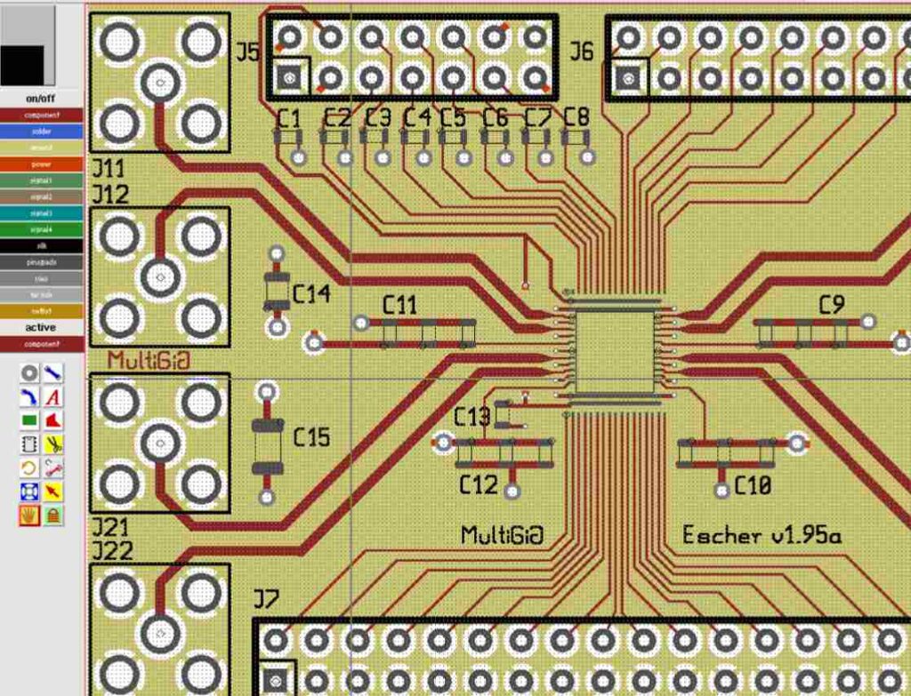
Here are some best practices to follow when laying out an HF PCB:
- Define impedance-controlled routing layers, usually internal layers. Maintain impedance across these layers.
- Place HF components first, then route traces point-to-point as short as possible between them.
- Route HF traces orthogonally – avoid acute angles which reflect signals.
- Use curved/tapered trace corners instead of hard 90° angles.
- Create power “islands” around HF components to isolate noise from other sections.
- Use large ground plane fills on multiple layers for low impedance reference.
- Provide guard traces around HF traces to control EMI.
- Separate analog and digital sections to prevent coupling.
- Minimize the number of vias used, follow via placement guidelines.
- Run crosstalk simulations and optimize trace spacing as needed.
- Account for component placement effects with EM analysis.
- Follow any specific layout guidelines from IC manufacturers.
Paying attention to these considerations during layout helps achieve good signal integrity through the HF PCB. The next section covers some analysis techniques used to verify the HF design.
HF PCB Analysis
To confirm that the PCB layout meets performance requirements, various analysis techniques can be utilized:
Frequency Domain Reflectometry
Frequency domain reflectometry (FDR) analyzes impedance and reflections along traces. Any discontinuities or improper termination will be highlighted. FDR helps identify and fix impedance issues during design.
Signal Integrity Simulations
Time domain reflectometry (TDR) and S-parameters analysis using a vector network analyzer (VNA) verifies signal transmission through the traces. Eye diagram analysis confirms that the HF digital signals retain adequate shape and quality.
Electromagnetic Interference
Radiated and conducted EMI analysis ensures the board passes standard emission requirements. Near-field probes scan for hotspots. Radiated emissions are checked in an anechoic chamber.
Power Integrity
The supply network is analyzed under load to check for acceptable voltage ripple, transients, and resonances. This ensures steady, clean power for HF circuits. Plane resonance can cause power issues.
Antenna Analysis
Any trace, via, or component forming resonant structures could act as unwanted antennas, causing EMI. Simulation checks for unintentional trace antennas and coupling.
Thermal Analysis
Both electrical performance and component life are affected by heating. Thermal modeling identifies hotspots under worst-case power dissipation to evaluate cooling requirements.
Fixing issues found through analysis early in the design cycle helps avoid costly respins and delays further along in the project. The insights provided by simulation and measurement allow optimizing the design for the target frequency range.
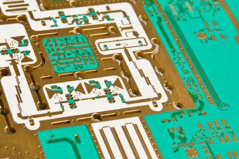
HF PCB Materials and Constructions
The materials and construction methods used for the PCB have a significant impact on achieving required HF performance. Here are some typical materials and constructions used:
Substrate Materials
Popular substrate materials include:
- PTFE (Teflon) – Lowest loss material, poor thermal conductivty
- Low-loss composite materials with ceramic filler
- Hydrocarbon ceramics – Cost-effective; moderate loss
- FR-4 (Glass epoxy) – Higher loss; lowest cost
PTFE is ideal for the most demanding RF applications. Ceramic-filled PTFE offers a good tradeoff of performance vs. cost. FR-4 is generally too lossy for wavelengths under 10-15cm.
Copper and Dielectrics
Thicker copper (2+ oz) minimizes skin effect losses. Thin dielectrics (5-10 mils) reduce parasitic capacitance but require finer lines to maintain 50Ω impedance. Medium thick dielectrics offer a compromise.
Copper Roughness
Standard “reverse treat” foil provides adequate performance up to ~10 GHz frequencies. Above that, “very low profile” (VLP) foils with lower roughness help limit conductor losses at mmWave bands.
Prepregs
Prepreg materials bond the copper foil to core substrate materials. They impact dielectric performance. Most common types include 170°C, 180°C, or 200°C Tg materials with low Df.
Layer Stackup
The layer stackup arrangement minimizes thickness deviations from the center-line axis for better impedance control. Core thicknesses are often multiples of prepreg thicknesses.
Via Construction
There are three main types of via construction:
- Through hole – Low cost, but presents impedance discontinuity
- Blind – Only connects inner layers, allowing uninterrupted outer plane
- Buried – Connects inner layers without reaching outer layers
Blind/buried vias minimize discontinuities in ground planes for best HF performance. Microvias (0.10-0.15mm) are used for highest frequencies.
Surface Finishes
ENIG (Electroless nickel, immersion gold) offers the best surface for HF circuits. HASL (Hot air solder leveling) is lower cost but can cause solder fillets which impact impedance. Other finishes like Immersion Silver or OSP (Organic Solderability Preservative) provide intermediate performance/cost.
High Density Interconnects
To fit routing dense ICs, traces can be narrowed or substrates thinned. Backdrilling (removing stub portions of unused vias) and staggered vias help.Sequential lamination combines multiple routing layers.
Embedded Components
Passives, resistors and other components can be formed within the PCB layers. This saves space while minimizing parasitics. Discrete components can also be embedded into the board.
Applications of HF PCBs
There are many applications and products that rely on properly designed HF PCBs:
- Wireless Communications – Cell phones, WiFi, Bluetooth. Circuits like power amplifiers, mixers, filters, antenna elements.
- Radar and Navigation – Air traffic control, weather radar, aircraft avionics. Fast data acquisition and processing.
- High-Speed Computer Interfaces – PCIe, USB 3.0/4.0, HDMI. Multi-gigabit serial data transmission.
- Microwave Radio Links – Backhaul networks. Circuits like mixers and multipliers.
- SATCOM – Satellite communications. Circuits like upconverters, downconverters, modulators.
- Medical Imaging – MRI, PET, and CT scanners. Rapid waveform generation and sampling.
- Wireless Power Transfer – Transmitting power wirelessly via RF energy. Careful impedance control.
- Automotive Sensors – Short range radar and LIDAR for collision detection and avoidance.
- 5G Networks – Next generation cellular infrastructure at mmWave bands.
- Aerospace/Defense – Phased array radars, electronic warfare systems, missile guidance. Ruggedized construction.
This list highlights the wide range of applications enabled by advanced HF PCBs operating into the multi-GHz frequency range.
HF PCB Fabrication and Assembly
Fabricating an HF PCB requires great precision to meet tight electrical tolerances. Here are some key PCB fabrication and assembly processes for HF boards:
Lamination
Layers are precisely aligned and laminated using high pressures and temperatures. This ensures minimal thickness variation across layers, critical for impedance control.
Drilling
Laser direct imaging (LDI) photoplots provide excellent hole registration. Tight tolerance mechanical and laser drills create vias. Entry/exit delamination must be prevented.
Plating
Electrolytic copper plating must deposit uniform thickness in holes. Smart plating solutions improve throwing power. Surface finishes are applied uniformly.
Etching
Printed circuit patterns are etched from copper sheets. Tight process controls prevent over/under-etching which affects trace impedances.
Testing
Rigorous electrical testing checks for shorts, opens, impedance, propagation delay, insertion loss, noise, crosstalk and functionality.
Soldering
For assembly, reflow ovens provide careful temperature profiling. Hand soldering requires skilled operators. Cleaning removes residues.
Challenges of HF PCBs
While providing tremendous capabilities, HF PCBs come with unique challenges including:
- Extreme sensitivity to layout, construction and materials
- Narrow processing windows – small defects can cause failure
- Simulation complexity due to signal integrity issues
- Technically demanding fabrication and assembly
- High development costs and lead times
- Limited fabricator and assembler options for advanced boards
- Difficult troubleshooting and repair after assembly
- Steep learning curves for designers unfamiliar with HF
These factors make it essential to partner with fabricators and assemblers who specialize in advanced HF PCB technologies. Their expertise in HF processes, simulation, testing and troubleshooting are critical for success.
The Future of HF PCBs
HF PCB technology continues advancing to meet the needs of emerging applications:
- Higher Frequencies – PCBs moving into the mmWave region, above 30 GHz. Enables applications like 5G networks, self-driving vehicles.
- Embedding – More integration of components into board layers. Saves space while improving electrical performance.
- Miniaturization – Continued progress towards smaller features, finer lines and spaces, microvias. Higher component densities.
- New Materials – Lower-loss, tighter Dk tolerance substrates for improved performance.
- Multilayer Construction – Complex designs with 20+ layers for routing dense ICs. Built-up technologies.
- High-Speed Design – Supporting data rates above 50 Gbps. Careful channel modeling and equalization techniques.
- Modeling Improvements – More accurate modeling of loss characteristics. Better design convergence through multiple iterations.
- Automation – Use of AI for improved layout optimization. Reduced development time.
- Testing – New techniques for on-board characterization to supplement modeling.
- Flexible/Additive Mfg – DD PCB fabrication techniques for prototypes and low volume.
By leveraging these advancing technologies and design practices, HF PCBs will continue improving in capability and performance to power leading-edge electronic systems.
Summary of Key HF PCB Considerations
To summarize, here are the key considerations when designing and manufacturing high frequency PCBs:
- Analyze designs from DC up to highest operating frequency
- Controlled impedance along entire signal path
- Minimize parasitics – self/mutual capacitance and inductance
- Use lowest loss materials possible – substrate, copper, etc.
- Plan stackup arrangement for symmetry, isolation
- Keep traces short – less than 1/10 wavelength
- Use minimal vias; manage their placement carefully
- Provide robust power distribution network
- Use multiple low-impedance ground/reference layers
- Isolate analog and digital sections
- Perform crosstalk analysis; optimize trace spacing
- Run EM simulations to predict performance
- Follow stringent fabrication and assembly processes
- Perform comprehensive testing and characterization
Paying attention to these HF guidelines helps achieve first-pass success and reliable operation at gigahertz frequencies and beyond.
Frequently Asked Questions
Here are some common questions about high frequency PCBs:
What are some typical applications of HF PCBs?
HF PCBs are used in wireless communications, radar systems, satellite technology, medical imaging equipment, high-speed computer interfaces, aerospace/defense electronics and automotive sensors. Essentially any application involving high frequency signals from hundreds of MHz to tens of GHz.
At what frequencies do PCBs start being considered high frequency?
There is no exact threshold, but typically PCB operating frequencies above a few hundred MHz begin to have HF considerations. Wavelength becomes short enough that proper HF layout techniques are needed.
What fabrication processes are most critical for HF PCBs?
Lamination, drilling, plating, etching and testing require tight tolerances and standards for HF PCBs. Any defects can degrade performance. Some specific processes like sequential lamination may also be used.
How are simulations used for HF PCB design?
Simulations like FEM, FDTD, and circuit modeling are critical to predict HF PCB performance prior to fabrication. They help identify and address issues with reflections, impedance mismatches, parasitics and EMI early in the design cycle.
Why is impedance control important for HF PCBs?
Controlled impedance traces match circuit impedances to minimize harmful reflections along the transmission path. This allows the signals to propagate efficiently without distortion at high frequencies.
What construction approaches help minimize parasitics?
Keeping traces short, proper grounding/isolation, blind/buried vias, backdrilling unused vias, ground planes close to signal layers all help reduce parasitic components which interfere with signals.
Conclusion
In summary, high frequency PCB design requires special considerations in layout, stackup, materials, simulations, fabrication and testing to


