PCB Design Files (Gerber Files, ODB++, etc.)
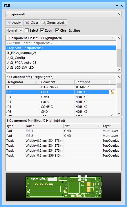
The most critical piece of documentation for PCB manufacturing is the design file. This is the original CAD data that defines the copper layers, drill holes, board outline, solder mask, silkscreen, and other features of the bare board. There are a few common formats for outputting PCB design files:
Gerber Files
Gerber is the most widely used data format for PCB designs. It is a vector image file format that describes each layer of the board in a series of coordinates and draws. A complete set of Gerber files should include:
- Copper layers (e.g. Top Layer, Bottom Layer, Inner Layers)
- Solder mask layers
- Silkscreen layers
- Drill files (Drill Drawing, Drill Guides)
- Profiling data (Board Outline)
Most PCB design tools can export Gerber files. You’ll need to configure the export settings to ensure all necessary layers are included at the appropriate resolution.
ODB++
ODB++ (Open Database++) is a newer, intelligent CAD format that is gaining adoption. Unlike Gerber which is a collection of “dumb” image files, ODB++ includes rich metadata about the PCB design such as layer types, nets, materials, and more.
The main benefits of ODB++ are:
- All design data is contained in a single file database
- Intelligent data allows for more automated analysis and processing
- Supports embedded components and advanced packaging
If your CAD tool and manufacturing partners support it, ODB++ can help streamline the handoff from design to fabrication. However, Gerber is still the most common and universal format.
IPC-2581
IPC-2581 is an open, vendor-neutral data exchange format for PCBs. Similar to ODB++, it contains intelligent design data in an XML-based format. It was developed by the IPC (Association Connecting Electronics Industries) to improve interoperability between different tools.
While a promising format, IPC-2581 has not yet seen widespread industry adoption compared to Gerber and ODB++. But it is an option to consider if your toolchain supports it.
Bill of Materials (BOM)
The bill of materials or BOM is a list of all the components that will be placed on the PCB. At a minimum, the BOM should include for each component:
- Reference Designator (e.g. R1, C2, U1)
- Manufacturer Part Number (MPN)
- Description
- Quantity
Additional data that is helpful to include:
- Manufacturer name
- Supplier name and part number
- Component package type and dimensions
- Alternative part numbers (in case the primary is not available)
The BOM may be provided in spreadsheet form (.xlsx) or as a comma-separated value (.csv) file. It’s important that the reference designators exactly match those used in the design files and assembly drawing.
| Ref Des | MPN | Description | Qty | Package |
|---|---|---|---|---|
| R1, R2 | RC0603JR-071KL | 1 kOhm resistor | 2 | 0603 |
| C1 | CL10B104KO8WPNC | 0.1 uF capacitor | 1 | 0603 |
| U1 | ATMEGA328P-AU | 8-bit MCU | 1 | TQFP-32 |
Assembly Drawing
The assembly drawing provides a visual reference for the component placement on the PCB. It typically includes:
- Board outline
- Component outlines
- Reference Designators
- Polarity indicators
- Additional assembly notes
The assembly drawing may be provided as a PDF or CAD drawing file (e.g. DXF, DWG). For simpler PCB designs, the assembly drawing information may be included on the silkscreen layer in the fabrication files.

PCB Stack-up Diagram
The stack-up shows the arrangement of copper and insulating layers in the PCB, along with their thicknesses and materials. It’s an important reference for the fabricator to ensure the board is built to spec.
A stack-up diagram should show:
- Number of layers
- Thickness of each layer
- Copper weights
- Dielectric material between layers
- Solder mask color and thickness
- Surface finish (e.g. HASL, ENIG)
This information may be included as a separate drawing or table in the fabrication files.
| Layer | Material | Thickness (mm) | Copper Weight (oz) |
|---|---|---|---|
| Top Solder Mask | LPI | 0.015 | – |
| Top Copper | Copper | 0.035 | 1 |
| Core | FR-4 | 0.200 | – |
| Bottom Copper | Copper | 0.035 | 1 |
| Bottom Solder Mask | LPI | 0.015 | – |
| Total Thickness | 0.300 |
PCB Test Specifications
Testing is an important step to verify the bare board and assembled PCB meet requirements. Providing clear test specifications helps avoid misunderstandings and ensures the delivered boards have gone through the appropriate validations.
Some common PCB Testing and validation steps include:
- Automated optical inspection (AOI)
- Electrical continuity and isolation testing
- Functional testing
- In-circuit testing (ICT)
- Burn-in testing
The test specification should detail which tests need to be performed and the pass/fail criteria for each. Any special test fixtures or procedures should also be spelled out.
Mechanical Drawings
For PCBs with unique mechanical requirements, additional drawings may be needed to convey things like:
- Mounting hole sizes and locations
- Keep-out areas
- Slots or cutouts
- Detailed board dimensions
- 3D views for complex geometry
These drawings provide a fabricator with the information needed to quote and manufacture any custom aspects of the board. Tolerances and materials should be specified as well.
Additional Documentation
Some other documentation that may be required depending on the project:
- Schematic diagrams
- Design rules and constraints
- Thermal management diagrams
- Signal integrity and power delivery network reports
- Packaging and shipping specifications
- Compliance and certification documents (e.g. RoHS, UL, CE)
The key is to provide as much relevant information upfront so your manufacturing partners have what they need to accurately quote, fabricate, assemble, and ship your boards.
FAQ
What if I’m missing some of the documentation?
If you don’t have all the files listed above, reach out to your PCB design engineer or CAD team. They should be able to generate the missing pieces from the original design data. If some documents simply don’t exist (like test specs), work with your manufacturer to determine what information they need to proceed.
Can I just provide Gerber files?
While Gerbers are the most important part, most manufacturers will require additional files like the BOM, assembly drawings, stack-up diagram, and test specs in order to provide a complete quote and build the board to your requirements. Gerbers alone don’t tell the whole story of what you need.
What if I need to make changes after I’ve submitted the files?
The ability to make changes depends on how far along in the process the board is. If fabrication hasn’t started, you can usually submit revised files. But there may be a cost impact for re-tooling. If production has already begun, changes are likely not possible without scrapping the current batch and starting over. Be sure to carefully review all documentation before signing off for production.
How do I know my manufacturer will follow my documentation?
Reputable PCB fabrication and assembly partners will always follow the provided specifications. If anything is unclear, they will ask for clarification before proceeding. You can also request first article inspection (FAI) reports and production samples to verify adherence to your specs. If a vendor deviates without authorization, that’s a big red flag.
What’s the best way to avoid documentation issues?
The best way to avoid issues is to start with a complete, accurate design package from your PCB designer. Use a PCB design review checklist to catch any errors or missing information before releasing the design. Archive all the design outputs and supporting documents in one place. And work closely with your manufacturing partners to make sure they have everything they need and understand your requirements fully.
Conclusion
PCB documentation is a critical part of the design-to-manufacturing handoff process. By providing a complete set of accurate design files, drawings, and specifications, you can ensure your boards are fabricated and assembled to your exact requirements.
The specific documents you need may vary depending on the complexity of the design and the processes used by your manufacturing partners. But at a minimum, be prepared to provide:
- PCB design files (Gerbers, ODB++, etc.)
- Bill of Materials (BOM)
- Assembly drawings
- PCB stack-up diagram
- Test specifications
With proper planning and communication, you can make sure your documentation package sets your PCB project up for success through fabrication, assembly, and delivery.
