Overview
Circuit boards, also known as printed circuit boards (PCBs), provide the foundation for virtually all electronic devices and equipment. They contain the conductive pathways or traces to interconnect electronic components and enable the flow of power and signals in a product. Circuit boards consist of multiple layers of different materials that are combined to provide the required electrical, mechanical, and thermal characteristics. This article provides an in-depth look at the various materials used to fabricate circuit boards by Rayming.
Circuit Board Substrate Materials
The substrate forms the core layer in a multilayer PCB providing mechanical support. The most common materials used are:
FR-4 Glass Epoxy
FR-4 glass epoxy is the most popular substrate material used in over 90% of rigid PCBs. It consists of woven fiberglass cloth bonded with an epoxy resin matrix. The fiberglass reinforcement provides mechanical strength while the epoxy gives chemical resistance.
FR-4 offers a good balance of electrical performance, mechanical properties, heat resistance, cost and ease of manufacture. The dielectric constant (Dk) of FR-4 is around 4.5 with good thermal performance up to 130°C (Tg). It can support multilayer boards with up to 30 conductive layers.
CEM-1/CEM-3 Cotton Paper
CEM-1 and CEM-3 substrates consist of cellulose paper reinforced with cotton linters. They provide excellent dielectric performance with a low Dk of 3.5-3.9 and low Dissipation Factor.
They are well-suited for high frequency analog and RF circuits up to 6 GHz. However, moisture absorption is higher for paper-based laminates. CEM-1 (Tg 105°C) and CEM-3 (Tg 120°C) offer lower thermal capability than FR-4.
Polyimide
Polyimide laminates like Kapton provide superior thermal resistance up to 220°C and excellent dimensional stability across temperature swings. Polyimide has a Dk of 3.4-3.5.
Its flexible nature allows fabrication of flexible circuit boards. However polyimide substrates are more expensive than FR-4 and the material is difficult to machine or drill holes.
PTFE (Teflon)
PTFE or Teflon substrates provide extremely high temperature resistance of up to 280°C. PTFE has excellent electrical properties with a low Dk of 2.1.
It offers high chemical resistance and low moisture absorption. The disadvantages are high cost and inferior mechanical strength. Modified versions like glass fiber reinforced PTFE help improve the strength.
Others
Some other less common substrate materials include:
- BT (Bismaleimide-Triazine) resin: Dk of 3.8 and Tg up to 180°C
- Cyanate Ester: Dk of 3.5 and Tg over 180°C
- Ceramics like Alumina and Aluminum Nitride: High thermal conductivity
Circuit Board Outer Layers
The outer layers of PCBs serve as the interface for component mounting and provide the finest conductive traces for circuit interconnects. The common outer layer materials are:
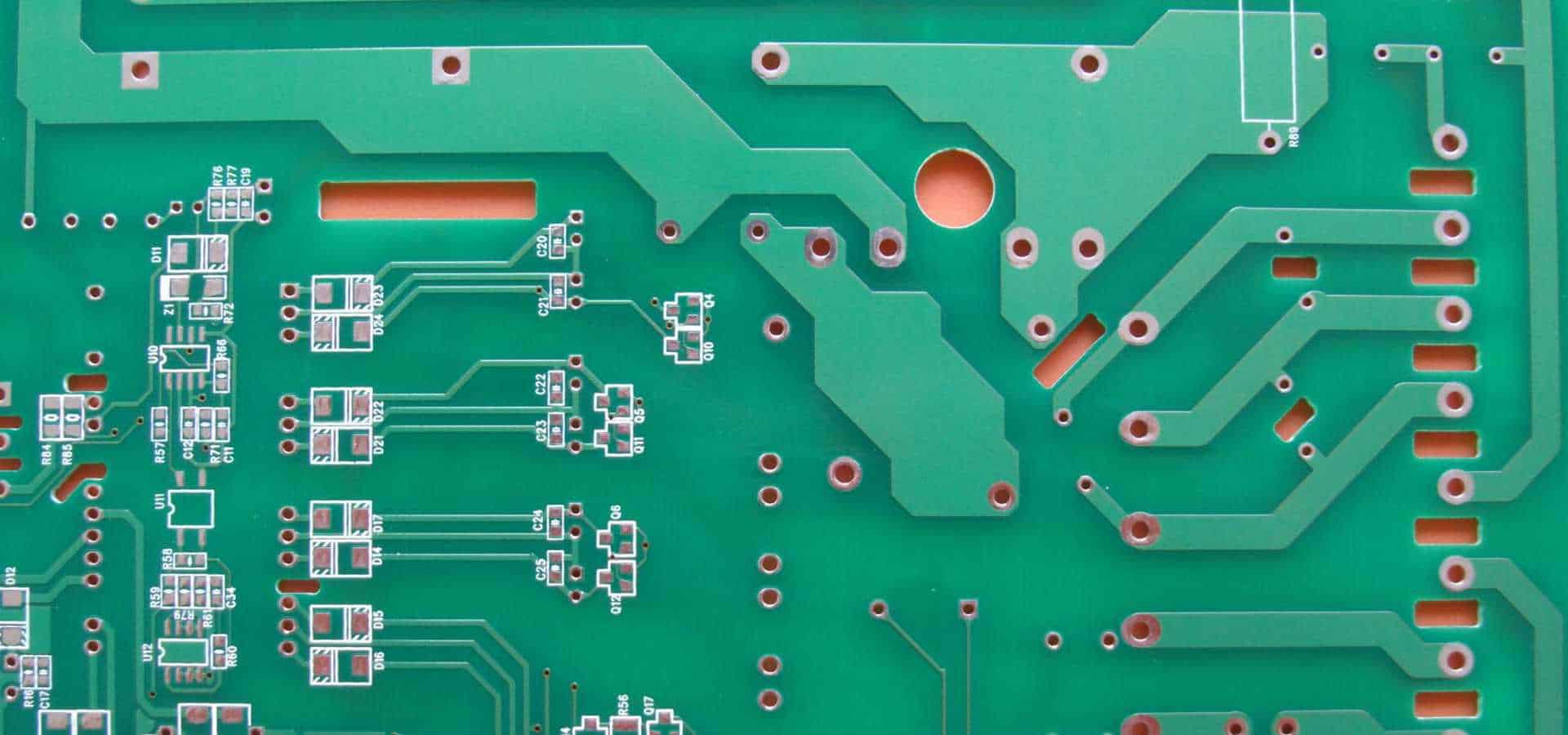
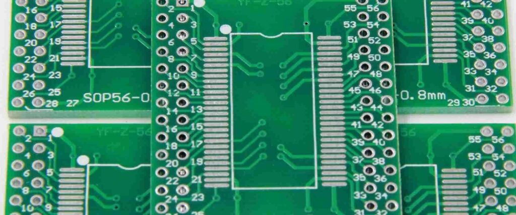
Copper Foil
Copper foil is universally used for PCB outer layers which interface with components and carry fine traces. Rolled copper or electrodeposited copper of 1⁄2 to 2 oz thickness is bonded to the substrate core using glass fiber reinforced epoxy prepregs.
1 oz (35 μm) copper foil is most common allowing finer 8 mil traces and adequate current carrying capacity. 2 oz (70 μm) copper provides higher current capacity but limits trace/space to 10 mil.
Very thin copper down to 9 μm with special treatments like VSP2 supports ultra-fine line PCBs with 2 mil trace/space.
Solder Mask
The solder mask (solder resist) is a polymer coating applied on the outer copper layers of a PCB wherever soldering is not desired. Green is the most common color. Solder mask protects the copper from oxidation and prevents solder bridges between pads.
Two types of solder mask used are Liquid Photo Imageable Solder Mask (LPISM) and Dry Film Solder Mask (DFSM). LPISM provides higher resolution down to 3 mil openings while DFSM allows faster processing.
Silkscreen Legends
Silkscreen printing applies epoxy-based permanent paints as legends on the PCB for component placement guides, product logo, board identification, polarity markers etc. Black legend prints on the solder mask provide good contrast.
Silkscreen inks withstand soldering heat and abrasion. Printing tolerance down to 4 mil line/space is achievable.
Surface Finishes
Surface finishes are applied to exposed copper pads and traces to facilitate soldering and prevent oxidation. Common finishes are:
- Organic Solderability Preservatives (OSP): Most economic but provide temporary protection.
- Immersion Tin: Provides good solderability but prone to whisker growth
- Immersion Silver: Excellent solderability and shelf-life with cost higher than OSP
- Electroless Nickel Immersion Gold (ENIG): Most reliable and robust finish
Multilayer Stackup in Circuit Boards

Multilayer PCBs consist of alternate layers of conductive copper and insulating dielectric bonded together into a monolithic structure.
Two construction approaches are used:
Subtractive Process
In the subtractive process, the core substrate is fully coated with copper on both sides. The unwanted copper is etched away to form the traces in the outer layers.
For inner layers, adhesiveless laminates like FR-4 are coated with copper using electrodeposition and then etched to create the desired copper pattern.
The core, inner layers and prepregs are stacked and laminated together. Mechanical drilling forms the plated through holes (PTH) providing interconnects between layers.
Additive Process
In the additive or semi-additive process, copper traces are built up only in the desired areas without the need for etching. This avoids wastage of copper.
A thin blanket copper layer is deposited on the core substrate. A photoresist coating is applied and patterned, exposing the areas for copper traces. Electroplating then builds up the copper thickness only in these exposed areas.
The additive process provides finer 4/4 mil trace/space capability. It is especially suited for HDI boards but involves more process steps.
Circuit Board Bonding Materials
Bonding materials are used to attach the layers together into a multilayer board:
Prepreg
Prepreg consists of glass fabric reinforcement impregnated with partially cured FR-4 epoxy resin. It is sandwiched between the copper foil and core substrate and cured under heat and pressure to bond them together. Prepreg provides adhesion as well as electrical and thermal insulation between layers.
The resin content and flow characteristics of prepreg enable filling of gaps during lamination while providing adequate copper bond strength.
Bonding Film
Bonding films are used as an alternative to prepreg for attaching layers in high density multilayer boards. LCP (liquid crystal polymer) bonding films offer very low Dk and Df allowing 3-10x enhanced signal speeds compared to prepreg.
Another advanced bonding material is Ajinomoto Build-up Film (ABF) that consists of thermoset polymers reinforced with glass fibers. ABF bonding enables finer pitch signal layers.
Plated Through Hole (PTH) Interconnections
Plated through holes (PTHs) are drilled holes with metal plating to provide electrical connections between various conductive layers in the PCB. The typical PTH stackup consists of:
Hole Drilling: Holes with diameter typically 12-25 mil are mechanically drilled through the PCB stackup using multi-spindle drill machines. The position and size are optimized for component pins and vias.
Deburring: A chemical deburring process removes debris from hole drilling and cleans the hole walls.
Seed Layer Deposition: To enable copper electroplating, a thin seed layer of palladium or electroless copper is deposited over the hole walls.
Copper Plating: Electrolytic copper with thickness 25-40 μm is plated uniformly over the hole walls to metallize the PTH. Copper provides high conductivity.
Plating Resist: A dry film or liquid photo-resist coats over the entire PCB. It is imaged to expose only the PTH areas.
Outer Copper Plating: Electrolytic copper thickness of 25 μm is plated over the PTH to form the outer pad connections.
Tin-Lead Plating: A thin solder plating of tin-lead may be applied to protect the copper surface from oxidation.
Resist Stripping: The plating resist is then chemically stripped away. This completes the PTH formation.
Common Materials Summary
The key materials used in different parts of typical circuit boards are:
| Location | Materials Used |
|---|---|
| Substrate Core | FR-4, CEM-1, CEM-3, Polyimide |
| Outer Layers | Copper Foil, Solder Mask, Silkscreen Legend |
| Multilayer Bonding | Prepreg, Bonding Film |
| Plated Through Holes | Copper Plating, Tin-Lead Plating |
Advanced Materials for Next-Gen Circuit Boards
While standard FR-4 PCB technology serves most applications today, new material alternatives are being developed:
Low Loss Materials
Low loss laminates like PTFE, Polyimide allow higher frequency operation above 10 GHz for emerging microwave and mmWave circuits.
High Thermal Conductivity
Laminates with ceramic fillers like Alumina, AlN provide 10-20X better thermal conductivity to manage heat in high power boards.
Embedded Components
Capacitors, resistors and inductors are being embedded inside PCBs using materials like glass microfiber films to achieve system miniaturization.
Stretchable Substrates
Novel elastomeric materials allow fabrication of stretchable flexible PCBs for wearable electronics.
Biodegradable Materials
Biodegradable substrates based on cellulose, lignin, and soy protein are being developed for environmentally friendly PCBs.
Additive Manufacturing
R&D is ongoing on novel additive processes to 3D print circuit boards using conductive and dielectric inks.
Thus continued materials innovation is poised to unlock newer PCB capabilities and applications.
Conclusion
Circuit boards consist of an intricate combination of conductive, insulating and bonding materials to provide the foundation for electronic systems. While FR-4 fiberglass-epoxy remains the workhorse material for most PCBs, newer alternatives are emerging for specialist requirements like high frequencies, thermal management, flexibility and embedded passives. Developments in additive manufacturing may enable on-demand 3D printed circuit boards. By leveraging both proven and emerging materials, circuit board technologies will continue to advance hand-in-hand with innovations in components and devices being integrated onto them.
Frequently Asked Questions
Q1. What is the most common base material used for circuit boards?
The most common base material is FR-4 fiberglass reinforced epoxy, which provides a good balance of electrical performance, mechanical strength, heat resistance and cost. It is used in over 90% of PCBs.
Q2. What materials are used for the outer layers of circuit boards?
The outer layers use copper foil for traces and component pads, solder mask to cover exposed copper, and silkscreen legend printing to indicate component placements, markings, logos, etc. Surface finishes like ENIG or immersion silver are applied on the exposed copper for soldering.
Q3. How are the layers bonded together in multilayer circuit boards?
Multilayer PCBs use prepreg – partially cured fiberglass-epoxy sheets that are sandwiched between layers and laminated under heat and pressure to bond them together. Advanced bonding films are also being used.
Q4. What materials are used to create plated through hole connections?
PTHs use electroplated copper over a thin seed layer to metallize the hole walls. A tin-lead plating may be applied to protect the copper surface from oxidation and improve solderability.
Q5. What new materials are being developed for advanced circuit boards?
Advanced materials being developed include low loss laminates, thermally conductive substrates, stretchable films, biodegradable materials, and inks for 3D printing of circuit boards.


