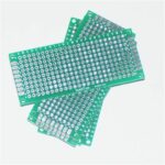
Introduction to PCB Visualization
PCB visualization is a crucial aspect of the printed circuit board design and manufacturing process. It allows designers, engineers, and stakeholders to visually represent and communicate the various aspects of a PCB, from the initial concept to the final product. By leveraging advanced visualization techniques and tools, businesses can streamline their PCB Development process, improve collaboration, and ensure high-quality results.
In this article, we will explore the importance of PCB visualization and how it can be effectively implemented throughout the entire business process. We will discuss the different types of PCB visualizations, their applications, and the benefits they offer. Additionally, we will provide insights into the latest tools and technologies used for PCB visualization and how they can be integrated into existing workflows.
The Role of PCB Visualization in the Design Process
Concept Visualization
The first step in the PCB design process is concept visualization. This involves creating a visual representation of the initial idea or concept for the PCB. Concept visualization helps designers and stakeholders to communicate their ideas effectively and ensures that everyone is on the same page from the start.
Some common techniques used for concept visualization include:
- Sketches and hand-drawn diagrams
- Digital wireframes and mockups
- 3D renderings and animations
By using these techniques, designers can quickly and easily convey their ideas and get feedback from stakeholders early in the process. This helps to identify potential issues and make necessary adjustments before moving on to the next stage of the design process.
Schematic Visualization
Once the concept has been finalized, the next step is to create a schematic diagram of the PCB. A schematic is a graphical representation of the electrical connections and components that make up the PCB. It provides a clear and concise overview of the PCB’s functionality and helps designers to identify potential issues before moving on to the physical layout.
Schematic visualization typically involves using specialized software tools that allow designers to create detailed diagrams of the PCB’s electrical connections. These tools often include libraries of common components and symbols, making it easy to create accurate and standardized schematics.
Some popular schematic visualization tools include:
- Altium Designer
- KiCad
- Eagle CAD
- OrCAD
By using these tools, designers can create detailed and accurate schematics that serve as the foundation for the physical layout of the PCB.
Layout Visualization
Once the schematic has been created, the next step is to create the physical layout of the PCB. The layout determines the placement of components and the routing of traces on the PCB. Layout visualization is crucial for ensuring that the PCB meets all the necessary requirements, including size, shape, and functionality.
Layout visualization involves using specialized software tools that allow designers to create detailed 2D and 3D models of the PCB. These tools often include features such as automatic routing, design rule checking, and simulation capabilities to ensure that the PCB meets all the necessary requirements.
Some popular layout visualization tools include:
- Altium Designer
- KiCad
- Eagle CAD
- Cadence Allegro
By using these tools, designers can create detailed and accurate layouts that ensure the PCB will function as intended and meet all the necessary requirements.
PCB Visualization in the Manufacturing Process
Manufacturing Visualization
Once the PCB design has been finalized, the next step is to move on to the manufacturing process. Manufacturing visualization involves creating visual representations of the various stages of the manufacturing process, from the initial prototyping to the final assembly.
Manufacturing visualization typically involves using specialized software tools that allow manufacturers to create detailed 3D models of the PCB and simulate the manufacturing process. These tools often include features such as virtual prototyping, assembly planning, and process optimization to ensure that the manufacturing process is as efficient and cost-effective as possible.
Some popular manufacturing visualization tools include:
- Siemens NX
- Dassault Systèmes DELMIA
- Autodesk Fusion 360
- Visicad
By using these tools, manufacturers can identify potential issues early in the process and make necessary adjustments to ensure that the final product meets all the necessary requirements.
Quality Control Visualization
Quality control is a critical aspect of the PCB manufacturing process. It involves ensuring that the PCB meets all the necessary quality standards and is free from defects. Quality control visualization involves creating visual representations of the various quality control processes, from the initial inspection to the final testing.
Quality control visualization typically involves using specialized software tools that allow manufacturers to create detailed 3D models of the PCB and simulate the various quality control processes. These tools often include features such as automated optical inspection (AOI), X-ray inspection, and functional testing to ensure that the PCB meets all the necessary quality standards.
Some popular quality control visualization tools include:
- Koh Young Technology
- Mirtec
- Viscom
- Saki Corporation
By using these tools, manufacturers can identify potential quality issues early in the process and make necessary adjustments to ensure that the final product meets all the necessary quality standards.

Benefits of PCB Visualization
Improved Collaboration
One of the key benefits of PCB visualization is improved collaboration between designers, engineers, and stakeholders. By using visual representations of the PCB, all parties involved in the development process can communicate more effectively and ensure that everyone is on the same page.
PCB visualization tools often include features such as real-time collaboration, version control, and shared libraries that allow teams to work together more efficiently. This can help to reduce errors, improve quality, and speed up the development process.
Faster Time-to-Market
Another benefit of PCB visualization is faster time-to-market. By using advanced visualization techniques and tools, businesses can streamline their PCB development process and bring products to market faster.
PCB visualization tools often include features such as automated design rule checking, simulation, and optimization that can help to identify potential issues early in the process and make necessary adjustments quickly. This can help to reduce the overall development time and bring products to market faster.
Cost Savings
PCB visualization can also lead to significant cost savings for businesses. By using advanced visualization techniques and tools, businesses can identify potential issues early in the process and make necessary adjustments before moving on to the manufacturing stage.
This can help to reduce the overall cost of development by minimizing the need for costly revisions and rework. Additionally, by using PCB visualization tools to optimize the manufacturing process, businesses can reduce the overall cost of production and improve their bottom line.
Improved Quality
Finally, PCB visualization can lead to improved quality of the final product. By using advanced visualization techniques and tools throughout the development process, businesses can ensure that the PCB meets all the necessary requirements and is free from defects.
PCB visualization tools often include features such as automated design rule checking, simulation, and quality control that can help to identify potential quality issues early in the process and make necessary adjustments. This can help to ensure that the final product meets all the necessary quality standards and is free from defects.
Conclusion
In conclusion, PCB visualization is a crucial aspect of the printed circuit board design and manufacturing process. By using advanced visualization techniques and tools throughout the entire business process, businesses can streamline their development process, improve collaboration, and ensure high-quality results.
From concept visualization to manufacturing and quality control, PCB visualization plays a critical role in ensuring that the final product meets all the necessary requirements and is free from defects. By leveraging the latest tools and technologies, businesses can realize significant benefits, including improved collaboration, faster time-to-market, cost savings, and improved quality.
As the demand for high-quality and reliable PCBs continues to grow, the importance of PCB visualization will only continue to increase. By investing in advanced visualization techniques and tools, businesses can stay ahead of the curve and deliver innovative and reliable products to their customers.
Frequently Asked Questions (FAQ)
-
What is PCB visualization?
PCB visualization refers to the process of creating visual representations of printed circuit boards (PCBs) throughout the design and manufacturing process. It involves using specialized software tools to create detailed 2D and 3D models of the PCB, simulate various processes, and communicate design intent and requirements to all stakeholders involved in the development process. -
Why is PCB visualization important?
PCB visualization is important because it helps to streamline the development process, improve collaboration between teams, and ensure high-quality results. By using visual representations of the PCB, designers, engineers, and stakeholders can communicate more effectively, identify potential issues early in the process, and make necessary adjustments before moving on to the manufacturing stage. -
What are some common PCB visualization techniques?
Some common PCB visualization techniques include sketches and hand-drawn diagrams, digital wireframes and mockups, 3D renderings and animations, schematic diagrams, and detailed 2D and 3D layouts. These techniques are used at various stages of the development process to communicate design intent, identify potential issues, and ensure that the final product meets all the necessary requirements. -
What are some popular PCB visualization tools?
Some popular PCB visualization tools include Altium Designer, KiCad, Eagle CAD, OrCAD, Cadence Allegro, Siemens NX, Dassault Systèmes DELMIA, Autodesk Fusion 360, and VisCAD. These tools offer a range of features and capabilities, including schematic capture, PCB layout, 3D modeling, simulation, and manufacturing planning. -
What are the benefits of using PCB visualization in the manufacturing process?
Using PCB visualization in the manufacturing process can help to identify potential issues early on, optimize the manufacturing process, and ensure that the final product meets all the necessary quality standards. By using specialized software tools to create detailed 3D models of the PCB and simulate various manufacturing processes, manufacturers can reduce the overall cost of production, improve efficiency, and ensure high-quality results.
| PCB Visualization Technique | Description | Benefits |
|---|---|---|
| Sketches and hand-drawn diagrams | Quick and easy way to convey initial ideas and concepts | Helps to communicate ideas effectively and get feedback early in the process |
| Digital wireframes and mockups | Digital representations of the PCB layout and design | Allows for easy sharing and collaboration between teams |
| 3D renderings and animations | Detailed 3D models of the PCB that can be rotated and manipulated | Provides a realistic representation of the final product |
| Schematic diagrams | Graphical representation of the electrical connections and components | Serves as the foundation for the physical layout of the PCB |
| Detailed 2D and 3D layouts | Precise models of the PCB that include component placement and routing | Ensures that the PCB meets all necessary requirements and functions as intended |

