Printed circuit boards (PCBs) are an integral part of most electronic devices and equipment. They provide the mechanical structure and electrical connections between components. PCB profiling or routing is the process of creating conductor traces on the board to connect components according to circuit design requirements.
V cut scoring is a technique used in PCB profiling to create breaks or gaps in the copper tracks on the board. It enables the PCB to be separated or segmented into smaller sections. The gaps created by V cut scoring facilitate the controlled snapping or breaking of the board along predefined lines. This article provides an in-depth look at V cut scoring – what it is, why it is done and how the cuts are made on PCBs.
What is Meant by V Cut Scoring
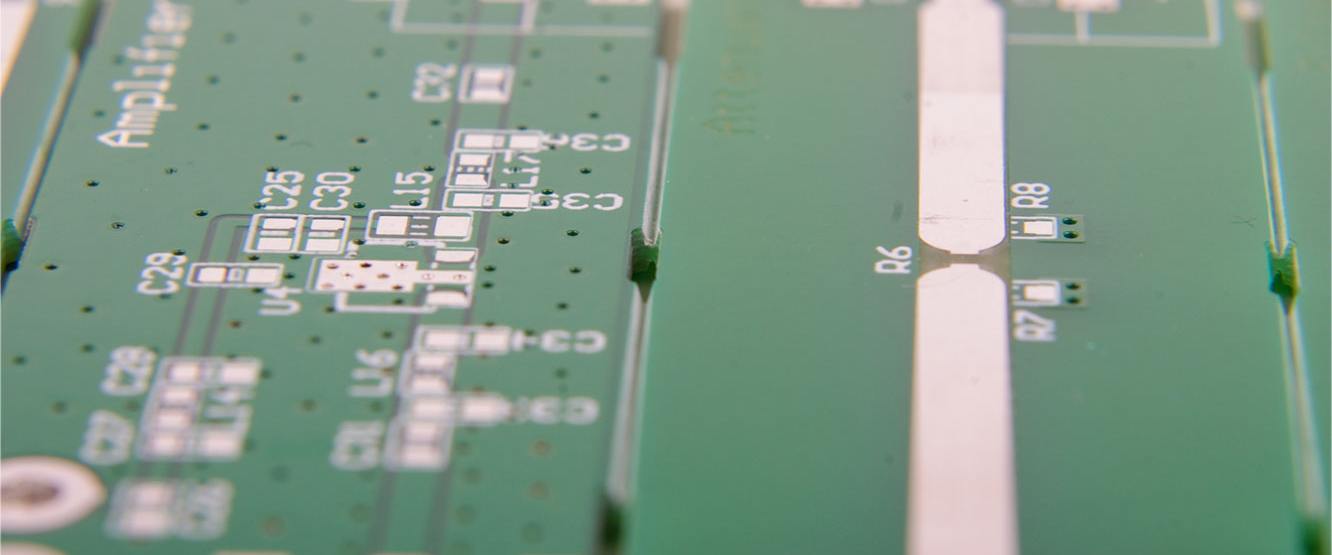
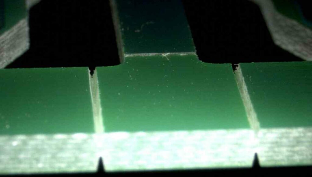
V cut scoring, also known as V-groove scoring or perfing, refers to making V-shaped cuts on a printed circuit board using mechanical or laser cutting methods. The cuts have a typical V-like cross-section and penetrate through the entire thickness of the copper layer. However, they do not completely cut through the entire PCB including the substrate.
The V cuts create a weak spot or stress point where the PCB can be snapped or broken easily and cleanly when pressure is applied. This allows the large PCB panel to be separated into smaller individual PCB units along the scored lines. The cuts may be made on one or both sides of the PCB depending on the separation requirements.
The V cut lines typically follow the board outline or the borders between adjacent PCBs on a panel. The width and depth of the V cuts can be controlled to achieve the desired snapping characteristics. Deeper and narrower V scoring allows cleaner breaking while broader cuts provide stress relief.
Why is V Scoring Done on PCBs?

V cut scoring provides the following benefits for PCB manufacturing and assembly:
- Panelization – V scoring enables efficient panel-based PCB mass production. Multiple small PCBs are arranged and fabricated together on a large panel which is later separated by breaking along the V cut lines.
- Singulation – It allows singulation or isolation of fabricated PCBs from the panel into individual boards and custom shapes. The scored lines serve as guides for accurate and clean separation.
- Segmentation – PCBs can be segmented into smaller sections for ease of assembly, testing or field replacement of parts using V cut outlines.
- Tooling features – The gaps created by V scoring can function as tooling features for holding or fixturing PCBs during assembly and inspection.
- Stress relief – V grooves help minimize mechanical stresses during PCB flexing. This reduces chances of copper tracks cracking.
- Impedance control – They can fine tune impedance in sensitive circuits by altering transmission line widths at V cut areas.
- Board thickness reduction – In multilayer boards, V scoring enables removal of materials to reduce thickness if required.
Profiling PCBs with V scores is a simple and efficient technique for facilitating panel-based manufacturing while also enabling flexibility and segmentation for assembly or field use.
How are V Cuts Made on PCBs?
V grooves are created on printed circuit boards using the following main methods:
Mechanical Scoring
Mechanical tools are used to cut or rout V-shaped grooves on the copper layers. Common techniques include:
- Saw cutting – High speed dicing saw blades make V notches along scoring lines. PCB panels are secured on worktables and the rotating blade is precisely aligned and fed to cut the required depths.
- Wheel cutting – A rotating V-shaped grinding wheel or cutter wheel similar to a router bit is used to mill the V grooves. The PCB is moved relative to the fixed cutting wheel to score lines.
- Die punching – Steel rule dies in V-shaped punch configuration are mechanically stamped onto PCBs to shear and indent V notches on the copper.
Mechanical V scoring provides a cost-effective means for high volume PCB scoring with the advantage of tactile feedback and easy depth control. However, the process can induce microcracks or copper burrs along cut edges.
Laser Scoring
Lasers rapidly vaporize copper to selectively ablate V-shaped grooves along the scoring lines. Laser systems provide fast, non-contact and highly accurate V cut profiling. Common laser scoring techniques include:
- CO2 lasers (10.6 μm wavelength) – CO2 laser beams are focused over the PCB path to directly remove copper and create V cuts. They allow high power density and deep penetration ideal for thicker boards.
- UV lasers (355 nm) – The small spot size and high resolution of UV lasers enable more precise and narrower V cuts. Low heat input minimizes damage. Well suited for sensitive, high density PCBs.
- Green lasers (532 nm) – Green lasers balance good small spot capabilities with high powers. They can ablate copper, laminates and solder masks for complete V groove formation in a single pass.
Laser systems enable fast prototyping and ramp-up with flexible software-controlled operations. Complex cut profiles are possible by CNC system integration. Heat affected zones are minimized for cleaner cuts compared to mechanical methods.
Cutting Comparison
Method | Advantages | Disadvantages —|— Mechanical Scoring | – Low cost equipment<br>- Mature processes<br>- Tactile feedback | – Copper burrs<br>- Microcracks<br>- Lower precision Laser Scoring | – Non-contact<br>- High speed<br>- High precision <br>- Low HAZ | – Higher equipment cost<br>- Limited depth control
Table 1: Comparison of mechanical and laser V scoring processes
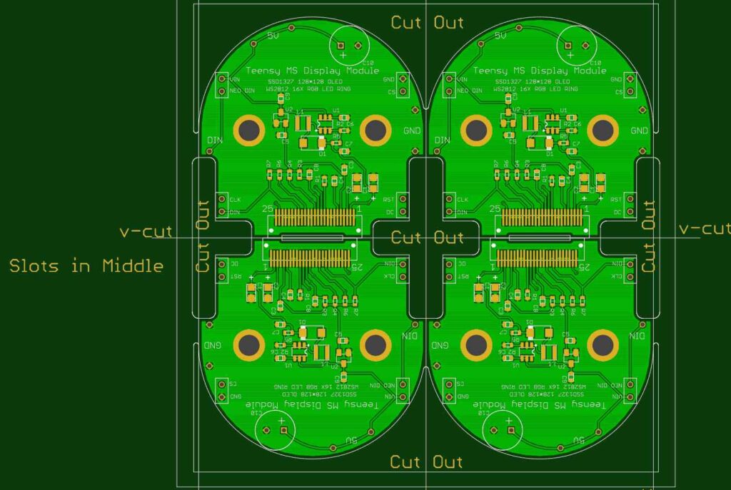
How are the Cuts Defined?
The V cut lines on the PCB are defined in the profiling or panelization stage of the design process. Based on the required segmentation and separation schemes, the cut profiles are outlined using CAD tools.
Key parameters defined for V scoring include:
- Scoring lines – Location and path of lines on the PCB layers. Outlines based on final board dimensions and break points.
- Cut depth – Penetration depth of the V notch through copper layers. Typically 50-80% of copper thickness.
- Cut width – Width of the groove at the top. Around 75-500 μm for mechanical and 50-100 μm for lasers.
- Cut angles – Angle of etched walls. 30 to 90 degrees.
Figure 2: V cut design – key parameters
The cut profiles are optimized to achieve reliable separation while minimizing undue PCB damage. The scoring data is integrated into the manufacturing process and transferred to the mechanical or laser cutting machines to create the V grooves accurately on the fabricated boards.
What are some Best Practices for V Cut Scoring?
Some guidelines and tips for effective V cut scoring on PCBs:
- Position V cuts precisely on the board outline to avoid clipping circuit features or components during separation. Maintain a minimum clearance.
- Frame or border cuts are recommended to isolate boards from panel edges to prevent premature edge breakage.
- Optimize cut depth and width based on PCB thickness and copper properties. Deeper cuts for rigid boards.
- Allow for sufficient web or uncut material between adjacent PCBs for panel integrity during handling and assembly.
- Incorporating stress relief features at cut terminations prevents propagation of cracks.
- Minimize number of cuts through high density PCB sections to reduce risk of short circuits.
- Avoid scoring over components or exposed conductors on assembly side of board.
- Symmetric cuts on both sides of board provide even stress distribution during separation.
- Testing and debugging initial V cut profiles on non-functional board areas first is recommended.
- Careful handling, stacking and storage of scored boards to prevent untimely breaking or cracking along V cut lines.
Applications and Examples
V scoring techniques are extensively used across many PCB implementations including:
Consumer electronics – ScoringAllows singulation of boards into individual devices from panels and shaping into non-rectangular forms.
Automotive – Creates snap-off sections for instrument cluster or engine control units for easy field repairs.
Aerospace – Thinner and lighter boards segmented by scoring to meet weight targets. Stress relief cuts prevent cracks.
Military – Facilitates fragmentation of circuits into smaller compartments for reliability enhancement.
RF/Microwave – Score lines tune impedance in sensitive RF circuits and antennas.
Medical – V grooves isolate circuits in body-worn devices to prevent current leaks across boards.
PCB suppliers offer V scoring services with capabilities to handle panel sizes up to 762 x 610 mm and thickness from 0.4mm to 6.4mm. Complex cut patterns, different V geometries and close cut tolerances of around ±0.025 mm are achievable with precision laser scoring systems.
FQA
Here are answers to some frequently asked questions about V cut scoring on PCBs:
Q: Can components and traces be present near V cut lines?
A: It’s recommended to keep cut lines away from components and traces, maintaining a minimum clearance of 0.2-0.5mm. If cuts need to pass components, laser ablation allows localized removal of solder mask first before scoring copper underneath.
Q: Does V scoring affect electrical performance?
A: Minor effects. The gaps can cause impedance changes in transmission lines. Narrow cuts minimize impact. Some coupling between circuits across cuts is possible. designers incorporate insulation gaps at cuts if needed.
Q: Are there limitations on V cut profiles?
A: Complex patterns are possible but curves and non-orthogonal lines increase fabrication time and cost. Avoid acute angles as they become weak points. High density boards have space constraints limiting cut paths.
Q: Can PCBs be edge plated after V scoring?
A: Yes, edge plating can be done. But the severed traces at V cuts will remain unplated unless a temporary bridge is added before plating to interconnect the segments.
Q: How are multilayer boards scored?
A: Multilayer PCBs are scored sequentially layer-by-layer to match cuts on all inner and outer layers. Aligned scoring is critical for proper separation without delamination or cracking.
Conclusion
V cut scoring is an indispensable technique in PCB manufacturing. It enables efficient panelization and singulation of boards while also providing means for segmentation and stress relief. The V notches can be created by mechanical methods or laser systems with laser ablation providing better quality and precision. Scoring parameters need to be optimized based on board specifications to achieve reliable separation without damage. V cut planning should account for assembly, handling and field use conditions to fully utilize its advantages. With growing circuit complexity, V cuts will continue to be critical for flexibly profiling PCBs.


