Introduction
A transparent printed circuit board, also called a see-through PCB, is a specialized type of board that allows visibility of components and traces embedded within the circuitry. While most standard PCBs use opaque insulating substrate materials, a transparent board utilizes clear materials that pass light.
Transparent PCBs enable unique applications in lighting, sensing, display, and other optics-related electronics. They also have novelty purposes and can provide an interactive experience for users to view the inner workings of a circuit board.
This article provides an in-depth look at how transparent PCBs are constructed and the applications, benefits, and technology trends driving adoption. We’ll examine methods to fabricate single, double, and multilayer transparent boards.
How are Transparent PCBs Constructed?
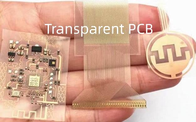
Fabricating a transparent printed circuit board requires specialized materials and processes to produce a clear insulating dielectric substrate that allows components to be seen through the board. Here are key methods used in transparent PCB construction:
Clear Substrate Materials
Standard opaque circuit boards use rigid FR-4 laminates or flexible polyimide films as the insulating dielectric substrate. Transparent PCBs require optically clear substrate materials that do not obstruct visibility, including:
- Transparent Polyimide – Flexible see-through polyimide film substrates are widely used. DuPont Kapton clear polyimide film provides excellent optical clarity.
- PMMA (Acrylic) – Rigid or flexible PMMA plastic substrates enable low cost transparent PCBs, but with lower thermal performance than polyimide.
- PET (Polyester) – Flexible clear PET films allow thin transparent flexible circuits. However, thinner PET can have low dimensional stability.
- Polycarbonate – Rigid optically clear polycarbonate substrates are an option, but are less common than polyimide or acrylic.
The transparent insulating substrate provides the foundation upon which the conductive copper traces and pads are fabricated.
Layer Fabrication
The fabrication process flow to build up transparent layers includes:
- Substrate Preparation – The transparent film or plate substrate is cleaned and prepared.
- Copper Lamination – Copper foil is carefully laminated onto one or both sides of the clear substrate.
- Photolithography – The circuit pattern is photoimaged and etched into the copper layer.
- Strip and Etch – Any protective photoresist is stripped off and the copper is fully etched.
- **Solder Mask ** – A clear solder mask may be screen printed or photodefined over the exposed copper.
- Legend Ink – Optional clear legend ink can identify components, traces, or text.
- Surface Finish – Transparent immersion tin or gold provide solderable surface finishes.
The result is a finished single or double-sided transparent circuit layer with the desired conductor pattern and solder pads protected.
Layer Stacking and Alignment
For multilayer PCBs, individual transparent layers are fabricated as outlined above, then precisely aligned and bonded together:
- Layer Alignment – Clear layers are optically aligned using windows or other fiducials.
- Bonding – Layers are laminated together using clear adhesive or thermoplastic bonding films.
- Via Formation – Vias are drilled through the layer stack and plated to form vertical interconnects between layers.
- Beveling – Optional beveled cutting of layer edges reduces internal reflections.
Great care must be taken when registering and bonding transparent layers to ensure minimal layer-to-layer misalignment which can obstruct visibility.
Final Assembly
After multilayer fabrication, components can be populated and assembled onto the transparent PCB:
- Component Loading – Place surface mount, socketed, and other components onto pads.
- Soldering – Reflow solder to electrically and mechanically attach components.
- Clear Conformal Coating – Optional transparent coating protects and insulates the assembly.
The assembled transparent PCB and components together form the completed circuit ready for installation and use in the end application.
Why Use a Transparent PCB?
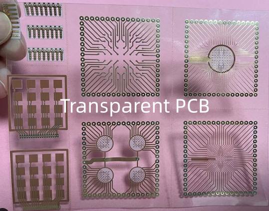
What are the key benefits and motivations for designers choosing transparent PCB technology versus standard opaque circuit boards?
Allow Component or PCB Light Emission
One of the primary uses of transparent PCBs is for light emission in LED boards and other luminaires:
- Edge-Lit LED Boards – LEDs mounted along the edge of the PCB emit light across the clear board.
- Backlit Overlays – Indicators, switches, and displays mounted on the transparent PCB are illuminated from behind.
- EL Wire/EL Panel Integration – Electroluminescent wires and panels can be embedded within a see-through board.
- Edge-Lit Acrylic Signs – Edge mounted LEDs transmit light through laser etched acrylic panels.
A transparent board construction allows light emission from sources mounted on or within the PCB itself.
Enable Component or PCB Visualization
Transparent substrates also enable direct visualization of components, traces, layers, and other features:
- Component Monitoring – View LEDs, resistors, and other components in operation.
- Trace/Layer Viewing – See embedded traces and layers within a multilayer PCB.
- Failure Analysis – Assist fault isolation by viewing internal board structure.
- Cooling Channel View – Observe flow through machined cooling channels.
- Assembly Verification – Confirm proper assembly with components visible.
The see-through construction provides a window into board operation and construction. This has functional benefits along with unique aesthetic appeal.
Expose Embedded Optical Elements
Specialized optical components can be integrated within a transparent PCB:
- Fiber Optic Routing – Optical fibers and waveguides are embedded within the layers.
- Sensor Integration – Transparent sensors like photodiodes can be die mounted onto the board.
- Light Pipe Channels – Send light horizontally across the PCB through light pipe structures.
- Edge Mounted Display – Small LCD or OLED displays are mounted along the board edge.
- Touch Panel Integration – Combine transparent capacitive touch sensing with other functions.
The transparency allows efficient transmission and manipulation of light across and through the PCB area.
Achieve Novel Visual Effects
Transparent boards also provide intriguing visual effects for applications like:
- Display Backlighting – Illuminate graphics, text, symbols on an overlay.
- Edge Glow Effects – Acrylic sheet edge glow with transparent PCB lighting.
- Artistic Circuits – Enable visual interaction and appeal.
- Academic Labs – Provide engaging way to view circuits for teaching electronics.
- Science Museum Displays – Interactive exhibits to highlight technology.
The see-through construction and visibility of electronics makes for engaging displays and user experiences.
Summary of Transparent PCB Benefits
- Enable light emission from LEDs, EL panels, and other illumination sources integrated into the PCB.
- Allow visualization of components, electrical traces, board layers, and other internal structures.
- Facilitate integration and operation of optical elements including fibers, sensors, light pipes, and displays.
- Create intriguing visual effects, art, exhibits, signage, and interactive experiences for users.
This wide range of benefits makes transparent PCB technology appealing for applications from lighting to academia to displayed electronics.
Industries Utilizing Transparent PCBs
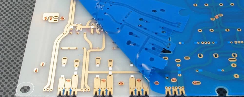
The benefits of transparent printed circuit boards are leveraged across many industries:
Lighting – Edge-lit LED boards, EL panel integration, and sign backlighting.
Academic Labs – Classrooms teaching electronics benefit from seeing circuitry.
Automotive – Interior display backlighting and center console illumination.
Gaming – Stylish illuminated motherboards and peripherals.
Consumer Electronics – Wearables, appliances, and gadgets using lighting effects.
Signage and Graphics – Backlit graphic overlays and edge-lit acrylic panels.
Industrial – Transparent touch panels integrated with HMIs and control electronics.
Medical – Monitoring operation of devices with visible electronics.
Museums & Science Centers – Interactive exhibits highlighting circuitry and technology.
Art & Decor – Unique applications leveraging visible glowing electronics.
This broad range of segments highlights the widespread applicability of transparent PCB technology.
Constructing Single-Layer Transparent PCBs
For simple circuits, a single-layer transparent printed circuit board may provide the ideal solution. Here is an overview of typical single-layer transparent PCB construction:
- Substrate – Polyimide, acrylic, PET or polycarbonate materials provide optically clear bases. Polyimide offers highest performance.
- Layer Thickness – Flexible substrates are typically 0.001” to 0.010” thick. Rigid materials from 0.040” to 0.250” thick.
- Copper Thickness – 1⁄2, 1 or 2 ounce copper foils are commonly used. Thicker copper reduces resistive losses.
- Patterning – Copper traces, pads, vias, and features are photoimaged and etched.
- Solder Mask – Optional clear solder mask lacquer protects exposed copper from oxidation.
- Coverlay – For flexible circuits, clear adhesive coverlay can insulate and protect conductors.
- Legends – Desired markings like component IDs, logos, or warnings printed in clear ink.
- Finishes – Immersion tin or gold provide solderable surface finishes.
Single-layer transparent PCBs enable simple lighting circuits and other straightforward designs with visual appeal.
Double-Layer Transparent PCB Construction
For increased circuit density, a double-sided transparent PCB sandwiches conductors between two substrates:
- Substrate Materials – Polyimide is commonly used, but also consider acrylic or polycarbonate. Match coefficients of thermal expansion.
- Conductor Layers – Double-sided offers two conductive copper layers which interconnect through plated holes.
- Vias – Holes drilled and plated to form conductive vias between layers. Layers are precisely aligned.
- Interlayer Bonding – Layers bonded using clear adhesive or thermoplastic bonding films.
- Finish – Immersion tin or gold provide solderable, corrosion resistant surface finishes.
- Solder Mask – Optional solder mask selectively coats the conductor patterns.
- Edge Bonds – Perimeter seals help prevent delamination at layer edges.
Double-sided transparent boards provide increased density with two conductive patterned layers interconnected by plated holes.
Multilayer Transparent PCB Construction
For more complex transparent PCBs, multilayer constructions over 4 layers are possible:
- Layer Count – Complex signal routing, power/ground, and shielding functions can benefit from additional layers. Common layer counts are 4, 6, and 8 layers.
- Sequential Lamination –Layers are fabricated individually then precisely aligned and laminated into a sandwich structure. Windows or fiducials aid alignment.
- Blind and Buried Vias – Blind vias connect inner layers to outer surface layers. Buried vias interconnect internal layers only.
- Fill Material – Optically clear via fill material indexes between transparent dielectric layers.
- Beveled Edges – Clear diagonal bevels cut into layer edges aids visibility and reduces internal reflections.
Multilayer transparent PCBs enable high density complex circuitry while maintaining light passage through the board. But fabrication complexity also increases.
Key Manufacturing Tolerances
Building transparent PCBs requires tight process control. Some key tolerances include:
- Layer Registration – Transparent layers must be precisely aligned, often to under 0.003” tolerance.
- Hole Size – Hole diameters must match pad sizes to within 0.001” to allow via plating.
- Hole Location – Drilled holes position relative to pads must be controlled to under 0.003”.
- Track Width – Conductors etched to specified widths within 0.001”.
- Track Spacing – Spacing between traces must be maintained to design.
- Surface Flatness – Minimal substrate warpage helps keep conductors in focus.
Maintaining these tolerances during fabrication is critical for transparency and function.
Trends Driving Adoption of Transparent PCBs
Some key trends are increasing demand and propelling adoption of transparent PCB technology:
MiniLED and MicroLED Displays – To backlight smaller higher density displays, transparent boards allow close interconnection with improved brightness control.
Haptic Feedback Integration – Combining transparent touch interfaces with haptics requires integration of these technologies within a PCB.
Multi-functional Integration – Interconnecting sensors, displays, lighting, and circuits drives multi-functional transparent boards.
IoT Edge Lighting – Transparent PCBs enable integration of sensors with indicator lighting in one IoT edge node.
Automotive Interior Lighting – Automotive human-machine interfaces are transitioning to illuminated transparent touch screens and control panels.
Wearable Technology – Lighting effects and displays are increasingly combined into smart watch bands, fitness sensors, and medical monitors.
As technologies continue converging, transparent PCBs will provide a platform for embedding diverse illumined electronics within a single device or system.
Summary of Transparent PCB Attributes
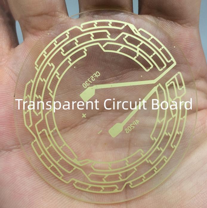
To summarize, here are the key characteristics of see-through printed circuit boards:
- Transparent substrate materials like polyimide, acrylic, and PET allow visible light passage.
- Photoimaging and etching precisely define conductive copper traces on the clear substrates.
- Multilayer sandwich constructions provide high density transparent electronics integration.
- Passive and active components can be selectively populated on the board.
- Lighting, sensors, optical fibers, and displays can be embedded within the transparent layers.
- Enables glowing lighting effects, component monitoring, and interactive experiences.
Continued improvements in fabrication and material quality will support broader adoption in illuminated electronics applications.
Frequently Asked Questions
Here are some common questions related to transparent PCB technology:
What limits the number of layers in transparent PCBs?
Alignment complexity and internal light attenuation or scattering limit practical transparent PCB constructions to 8 layers or fewer today. Research aims to enable multilayer stacking over 10 layers.
Does environmental robustness differ from standard PCBs?
Transparent boards offer comparable temperature cycling, vibration resistance, and reliability to traditional PCBs using the same base materials like polyimide or acrylic.
Are there any safety standards specific to transparent PCBs?
No universal safety standards exist yet, but transparent boards must still meet any product-specific regulations related to lighting, lasers, or optical devices.
What types of components can be used on transparent PCBs?
SMD devices including LEDs, ICs, resistors, connectors solder normally to a transparent board. Through-hole components can also be used with transparent hole plugging or selective opaque solder mask.
Can transparent circuits support high speed signals?
Polyimide-based transparent boards support multi-Gbps speeds. Low-loss materials are still in development to push microwave operation above 10 GHz.

