
A thermal printed circuit board (PCB) refers to a type of circuit board designed to conduct heat effectively away from components mounted on the board. As electronic devices shrink while power densities rise, carefully managing PCB temperatures becomes critical.
Thermal PCBs incorporate features to improve heat spreading across the board and facilitate transfer to external cooling structures. This prevents localized hot spots that can degrade performance, reduce reliability and cause failures.
In this comprehensive guide, we’ll explore what makes a PCB thermal, design elements to optimize thermal performance, types of thermal PCBs, selection considerations, installation and usage best practices. Let’s examine how thermal PCB technology enables the safe, reliable function of electronics.
What Makes a PCB Thermal?
A thermal PCB utilizes thermally conductive materials and heat flow structures to lower thermal resistance in the board. Common attributes include:
- Metal Core Substrate – Base metal layer conducts heat laterally across the PCB
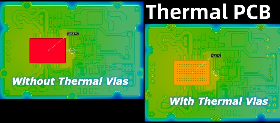
- Thermal Vias – Plated through holes channel heat between layers
- Thick Copper – Increased copper thickness lowers conduction resistance
- Copper Fills – Solid copper regions improve heat spreading
- Buried Planes – Inner ground/power planes act as heat spreaders
- Pad Reliefs – Cavities under pads connect to inner layers
- Extra Layers – Additional dielectric/copper layers increase conduction
- Attached Sinks – Aluminum heat sinks bonded to PCB
Thermal PCB with metal core, thermal vias, thick copper and attached heat sink
Importance of Thermal Management
Why is eliminating excess PCB heat so critical?
- Prevent Failure – Excessive temperatures degrade materials, delaminate boards and destroy components.
- Ensure Performance – Overheated components experience leakage currents and signal errors.
- Improve Reliability – Minimizing thermal cycling and gradients extends product lifetime.
- Allow Higher Power – Enables deployment of more power-hungry devices.
- Compact Design – Allows tighter spacing without overheating.
- Meet Safety Regulations – Satisfies maximum temperature requirements.
In short, thermal PCBs are vital for electronics functioning reliably within tight space constraints.
Thermal PCB Substrate Materials
The PCB substrate, or base material, determines thermal conductivity. Common options ranked:
- Aluminum – Highest thermal conductivity, most expensive
- Copper – Highly conductive, heavier than aluminum
- Alloy 42 – Iron-nickel alloy with good thermal characteristics
- FR-4 – Standard fiberglass PCB material, poor conductor
Additional substrate considerations:
- CTE – Matching coefficient of thermal expansion with mounted components
- Fabrication – Ease and cost of manufacture
- Weight – Density impacts finished PCB weight
Material choice involves tradeoffs between thermal performance, cost, and manufacturing factors.
Thermal PCB Substrate Constructions
Two main constructions exist:
Metal Core PCB
A base metal layer forms the core with dielectric buildup layers above and below onto which copper traces are formed. The thick metal core acts as a heat spreader.
Insulated Metal Substrate PCB
The metal base layer is covered on both sides by an insulating dielectric before copper patterning. This allows components to be mounted directly against the metal.
In both cases, the metal substrate is thicker than traditional FR-4 boards, from around 0.8mm to over 3mm.
Embedded Heat Slug Materials
Some thermal PCBs embed solid metal heat slugs/planes within the board layers:
- Copper – Excellent conductivity, matches PCB coefficient of thermal expansion
- Aluminum – Very high conductivity but CTE mismatch requires isolation
- Molybdenum – Compromise between conductivity and CTE match
The heat slugs provide low resistance localized heat removal beneath hot components.
Thermal Via Styles
Vias transferring heat between layers come in several styles:
Through Hole Vias
- Drilled holes spanning the entire board thickness
- Maximum heat conductance
Blind and Buried Vias
- Holes stopping at inner layers
- Conserve surface space but less vertical heat flow
Filled Vias
- Filling with conductive materials like solder or epoxy
- Reduces via thermal resistance
Microvias
- Small diameter vias, typically ≤ 0.15mm
- Allows higher via densities but thinner metal
Matching vias to design constraints optimizes vertical heat evacuation while minimizing fabrication challenges.
Copper Layer Usage
Copper distributes heat thanks to its high conductivity. Thermal PCBs maximize copper:
- Thicker copper – Reduces spreading resistance, typically >2 oz.
- Full layer copper fills – Solid pours increase heat spreading
- Additional layers – More dielectric/copper interfaces
- Buried planes – Inner ground/power layers act as heat spreaders
But more copper raises PCB fabrication costs. A balance must be struck.
Thermal Plane Construction Styles
| Plane Type | Description |
|---|---|
| Solid Plane | Continuous flat copper layer |
| Parallel Plane Slits | Narrow slots cut into plane |
| Hatched Planes | Network of orthogonal copper strips |
| Polygon Planes | Copper shapes with isolation gaps |
Split and hatched planes save copper but interrupt heat spreading.
Bonding Layers

Adhesives bonding layers impact thermal performance:
- Epoxy – Most common, moderate conductivity
- Acrylic – Higher conducting but more expensive
- Polyimide – Highly insulative, only when electrical isolation needed
Thinner bondlines reduce interface resistance but require more precise fabrication.
Solder Mask Openings
Removing solder mask over unused copper areas improves heat transfer to air:
- Exposed Copper – Bare copper has lowest thermal resistance
- Selective Deposition – Only coat high voltage areas
- Spot Exclusion – Keepouts around hot components
But exposes PCB to contamination and moisture ingress.
Attached Heat Sinks
Heat sinks bonded to PCB provide active cooling:
- Aluminum – Low cost, high conductivity
- Copper – Better performance but heavier and pricier
- Ceramic Filled Plastic – Electrically isolating but lower conductivity
Use thermally conductive epoxy, grease or solders to attach the sink.
PCB Edge Plating
Added metal plating along the PCB edge conducts heat:
- Copper – Highly conductive, readily bonds to PCB
- Nickel – Harder surface prevents wear
- Tin – Lower conductivity but easily solderable
Edge plating facilitates horizontal heat transfer to chassis.
Thermal PCB Design Factors
Factors to consider when engineering thermal PCBs:
- Component power and thermal profiles
- Temperature limits and deratings
- Thermal simulation results
- Layer counts and available space
- Routing constraints and isolation needs
- Mechanical stability and vibration resistance
- EMI shielding requirements
- Fabrication capabilities and costs
- Testability and inspectability
Analyzing all these aspects ensures an optimal thermal solution.
Thermal PCB Design Guidelines
Follow these guidelines when designing thermal PCBs:
- Position heat-sensitive components first
- Group high power parts together
- Assign thermally coupled items to same net
- Interleave heat sources and sinks
- Place thermal vias underneath hot parts
- Distribute vias evenly across board
- Align vias with anticipated heat paths
- Break up solid planes for isolation needs
- Request impedance modeling with extensive copper fills
- Verify thermal performance via simulations
- Include temperature sensors at key locations
Adhering to proven design practices prevents reliability issues.
Types of Thermal PCBs
Several classes of thermal PCB exist based on thermal requirements:
Type I – Basic Conduction
Modest enhancements to standard PCBs like thicker copper and filled thermal vias. Used for mild environments with simple conduction cooling needs.
Type II – Enhanced Spreading
Adds advanced cooling elements like metal core, exposed thermal layers and attached sinks. Handles tougher thermal loads.
Type III – High Power
Maximizes cooling capacity through features such as buried heat slugs, thermally optimized vias, and active cooling. Allows very high power densities.
Matching board thermal capabilities to the application prevents under or over engineering.
Thermal PCB Design Tradeoffs
| Benefit | Drawback | |
|---|---|---|
| Metal core substrate | Increased cost and weight | |
| Additional layers | Improved conduction | Fabrication challenges |
| Copper fills | Lowers thermal resistance | Limits routing capability |
| Exposed dielectric | Heat spreading to air | Contamination and moisture risks |
| Microvias | Allows greater densities | Reduces conduction and fill performance |
Optimized designs make appropriate tradeoffs to maximize thermal performance within constraints.
Thermal PCB Installation Best Practices
Follow these guidelines when installing thermal PCBs:
- Allow sufficient standoff height for airflow under board
- Ensure chassis contact areas are free of debris and oxidation
- Apply thermal interface material to chassis mating regions
- Use conductive surfaces and fasteners for grounding
- Firmly torque screws and retention hardware
- Electrically isolate board from chassis if needed
- Check for board bowing or warping after installation
- Verify thermal sensor readings post-assembly
Proper assembly and inspection prevents assembly issues and confirms the expected thermal performance.
Thermal PCB Selection Considerations
Factors to consider when selecting a thermal PCB design:
Thermal Loads
- Power levels and profiles of on-board components
- Temperature limits and derating requirements
Design Complexity
- Routing constraints and isolation needs
- Layer counts available
- Component spacing requirements
Performance Targets
- Temperature reduction goals
- Allowable thermal gradients across board
Mechanical Requirements
- Vibration resistance
- Shock withstand capability
- Structural stability
Fabrication Capabilities
- Partner abilities to produce designed features
- Lead times and costs
Analyzing requirements in all areas ensures an optimal thermal PCB solution.
Thermal PCB Usage Tips
Recommendations for successfully using thermal PCB technology:
- Actively cool – use fans/convection rather than just conduction
- Underfill high power components
- Apply thermally conductive epoxy under BGAs
- Ensure good contact between layers with low void lamination
- Avoid placing heat sources over board splits
- Monitor temperature sensors to validate performance
-Use thermal imaging to catch developing hot spots
- Qualify attachment processes like heat sink bonding
Verifying effectiveness through testing and inspection prevents issues.
Thermal PCBs – FQA
Here are answers to some frequently asked questions about thermal PCBs:
What limits the maximum power density achievable with a thermal PCB?
The ultimate limit comes from the total thermal resistance from junction to ambient and the allowable component temperatures. Practical limits also relate to fabrication capabilities, mechanical stability, electrical constraints, and system cooling capacity. But with optimal design, very high densities over 500 W/in2 are possible.
Is it better to use a few large or many small thermal vias?
For a given total via area, multiple smaller vias provide lower overall thermal resistance compared to one large via due to the increased surface area and perimeter. But dozens of tiny microvias pose fabrication challenges and reliability risks. A balance should be struck based on manufacturing capabilities.
Can thermal PCBs be reworked like standard PCBs?
While possible, reworking components on thermal boards is generally more challenging. Removal of large copper heat sinks or breaks in metal core substrates negatively impact thermal performance. Prioritize designs optimized for manufacturability rather than field serviceability.
How thick can copper layers be made on a thermal PCB?
There is theoretically no limit, but around 2 oz. copper is typically the maximum thickness used in fabrication. Extremely thick copper becomes functionally unwieldy and creates plating challenges driving up cost. Multi-layer builds with 2oz copper often achieve sufficient copper cross-section.
What limits the maximum operating temperature of a thermal PCB?
The lowest temperature rating of any material. This includes the substrate, bonding films, copper and dielectric properties. Ensure every component of the board stack can withstand expected thermal extremes without degradation.
Conclusion
Thermal PCB technology provides an indispensable means of managing heat dissipation as electronics shrink while power levels rise. By incorporating thermally engineered materials and structures, thermal PCBs conduct heat efficiently, prevent localized hot spots, and enable reliable operation. With careful analysis of thermal and electrical requirements along with fabrication capabilities, optimal thermal board solutions can be designed for even the most challenging application needs. Thermal PCBs form the foundation of effective electronics cooling.


