1. Cold Solder Joints
Cold solder joints are one of the most common issues encountered during PCB soldering. This problem occurs when the solder doesn’t melt properly, resulting in a dull, cracked, or grainy appearance of the joint. Cold solder joints can lead to intermittent connections or complete circuit failure.
Causes:
- Insufficient heat transfer from the soldering iron to the joint
- Contaminated or oxidized surfaces
- Inadequate flux application
- Improper soldering technique
Solutions:
- Use a higher wattage soldering iron or adjust the temperature
- Clean the surfaces with a desoldering braid or solder wick
- Apply fresh flux to the joint
- Ensure proper soldering technique (heating both components and applying solder simultaneously)
2. Solder Bridges
Solder bridges occur when excess solder creates an unwanted electrical connection between adjacent pads or traces on the PCB. This can cause short circuits, leading to malfunctions or damage to the board.
Causes:
- Excessive solder application
- Inadequate spacing between pads or traces
- Improper soldering technique
Solutions:
- Use a desoldering braid or solder wick to remove excess solder
- Ensure proper soldering technique (apply solder sparingly and with precision)
- Inspect the PCB design for adequate spacing between components
3. Dry Joints
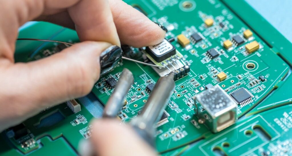
Dry joints, also known as cold solder joints, occur when the solder doesn’t flow properly and fails to create a secure connection between the component lead and the pad. This can cause intermittent or no electrical contact, leading to circuit failures.
Causes:
- Insufficient heat transfer
- Contaminated or oxidized surfaces
- Inadequate flux application
Solutions:
- Use a higher wattage soldering iron or adjust the temperature
- Clean the surfaces with a desoldering braid or solder wick
- Apply fresh flux to the joint
- Ensure proper soldering technique (heating both components and applying solder simultaneously)
4. Tombstoning
Tombstoning is a phenomenon where one end of a surface mount component (SMD) lifts off the PCB, forming a vertical or “tombstone” position. This can lead to poor electrical connections or complete circuit failure.
Causes:
- Uneven heating during the soldering process
- Excessive solder paste or solder volume
- Improper pad design or component positioning
Solutions:
- Use a soldering iron with a temperature-controlled tip
- Apply the correct amount of solder paste or solder
- Inspect the PCB design for proper pad layout and component footprints
5. Solder Balling
Solder balling is the formation of small, spherical balls of solder on the PCB or component leads. These solder balls can create unwanted short circuits or interfere with proper component placement.
Causes:
- Excessive solder application
- Contaminated or oxidized surfaces
- Improper soldering technique
Solutions:
- Use the correct amount of solder
- Clean the surfaces with a desoldering braid or solder wick
- Ensure proper soldering technique (heating both components and applying solder simultaneously)
6. Lifted Pads
Lifted pads occur when a pad or section of the copper trace separates from the PCB substrate. This can lead to complete circuit failure or intermittent connections.
Causes:
- Excessive heat during soldering
- Improper soldering technique
- Mechanical stress or impact on the PCB
Solutions:
- Use a lower wattage soldering iron and apply heat carefully
- Ensure proper soldering technique (avoiding excessive heat and mechanical stress)
- Consider repairing the lifted pad using conductive epoxy or wire jumpers
7. Overheated Components
Overheating components during the soldering process can cause permanent damage or failure. This can happen when excessive heat is applied for too long, or when components are not adequately protected from the soldering iron’s heat.
Causes:
- Improper soldering technique
- Using a soldering iron with excessive wattage
- Inadequate heat sinking or protection for temperature-sensitive components
Solutions:
- Use the appropriate wattage soldering iron for the job
- Apply heat judiciously and for the minimum time necessary
- Use heat sinks or shielding for temperature-sensitive components
8. Flux Residue
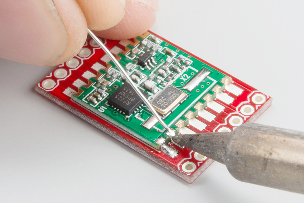
Flux residue left on the PCB after soldering can cause issues such as corrosion, electrical shorts, or interference with subsequent assembly processes.
Causes:
- Inadequate cleaning after soldering
- Using the wrong type of flux
- Improper cleaning procedures
Solutions:
- Clean the PCB thoroughly after soldering using appropriate solvents or cleaning solutions
- Use the recommended type of flux for the application
- Follow proper cleaning procedures specified by the PCB or component manufacturer
9. Delamination
Delamination is the separation of the layers within a multi-layer PCB. This can be caused by excessive heat, mechanical stress, or manufacturing defects, and can lead to circuit failures or intermittent connections.
Causes:
- Excessive heat during soldering
- Mechanical stress or impact on the PCB
- Manufacturing defects or quality issues
Solutions:
- Use appropriate soldering temperatures and techniques
- Handle the PCB with care to avoid mechanical stress
- Inspect the PCB for any manufacturing defects or quality issues
10. Cracked Solder Joints
Cracked solder joints can occur due to thermal cycling, mechanical stress, or improper soldering techniques. These cracks can lead to intermittent or complete circuit failure.
Causes:
- Thermal cycling (repeated heating and cooling)
- Mechanical stress or vibration
- Improper soldering technique (insufficient heat or solder)
Solutions:
- Use proper soldering techniques to ensure strong, reliable joints
- Minimize mechanical stress and vibration on the PCB
- Consider using stress-relieving materials or coatings for high-stress applications
11. Poor Hole-Fill
Poor hole-fill is a condition where the solder doesn’t completely fill the plated through-holes on the PCB, leaving voids or gaps. This can lead to intermittent connections or circuit failures.
Causes:
- Insufficient solder volume
- Improper soldering technique
- Contamination or oxidation in the plated through-holes
Solutions:
- Apply sufficient solder to completely fill the plated through-holes
- Ensure proper soldering technique (heating both components and applying solder simultaneously)
- Clean the plated through-holes before soldering to remove any contamination or oxidation
12. Solder Mask Damage
Solder mask damage can occur when the protective solder mask layer on the PCB is scratched, peeled, or damaged during soldering or assembly processes. This can lead to solder bridges, short circuits, or other issues.
Causes:
- Excessive heat during soldering
- Mechanical stress or impact on the PCB
- Improper handling or assembly procedures
Solutions:
- Use appropriate soldering temperatures and techniques
- Handle the PCB with care to avoid mechanical stress or impact
- Follow proper handling and assembly procedures to prevent solder mask damage
FAQ
- What is the difference between a cold solder joint and a dry joint? Cold solder joints and dry joints are often used interchangeably, but they refer to slightly different issues. A cold solder joint occurs when the solder doesn’t melt properly, resulting in a dull, cracked, or grainy appearance. A dry joint, on the other hand, occurs when the solder fails to flow and create a secure connection between the component lead and the pad.
- How can I prevent tombstoning during SMD soldering? To prevent tombstoning, ensure even heating during the soldering process by using a soldering iron with a temperature-controlled tip. Additionally, apply the correct amount of solder paste or solder, and inspect the PCB design for proper pad layout and component footprints.
- What should I do if I encounter lifted pads on a PCB? If you encounter lifted pads, consider repairing them using conductive epoxy or wire jumpers. However, if the issue is widespread or the repair is beyond your skill level, it may be better to replace the PCB entirely.
- How can I prevent flux residue issues after soldering? To prevent flux residue issues, clean the PCB thoroughly after soldering using appropriate solvents or cleaning solutions. Additionally, use the recommended type of flux for your application and follow proper cleaning procedures specified by the PCB or component manufacturer.
- What are the potential consequences of cracked solder joints? Cracked solder joints can lead to intermittent or complete circuit failure. These cracks can occur due to thermal cycling, mechanical stress, or improper soldering techniques. To mitigate this issue, use proper soldering techniques, minimize mechanical stress and vibration on the PCB, and consider using stress-relieving materials or coatings for high-stress applications.
