Introduction
Printed circuit boards (PCBs) integrate a wide array of electronic components and interconnects into a compact functional system. Ensuring the quality and reliability of PCB assembly requires thorough inspection to identify any defects introduced during the manufacturing process. Automated optical inspection (AOI) is commonly used but cannot visualize inside a PCB to detect issues like open vias or poor solder joints between hidden layers. For this purpose, X-ray inspection provides a powerful non-destructive internal view of PCB assemblies.
This article explores PCB X-ray inspection fundamentals, system components, image processing algorithms, design techniques, limitations, and comparisons to other inspection methods. We’ll examine how X-ray inspection fits within the overall PCB quality control workflow. Read on for an in-depth look at the benefits and implementation of X-ray imaging for electronics inspection.
Principles of X-ray Imaging
X-ray imaging utilizes high energy electromagnetic radiation to penetrate solid objects. As X-rays pass through matter, some radiation is absorbed based on material density and thickness. Denser areas like solder joints and conductor traces attenuate more X-rays, while low density regions allow increased transmission.
Placing a detector on the opposite side captures this selective attenuation information to produce a projected X-ray image. Contrast arises from relative absorption differences within the object. This allows visualizing the internal structure, like bone within soft tissue for medical scans.
For PCB inspection, X-rays reveal components, traces, and solder connections hidden within the board that optical systems cannot access. Voids, cracks, open vias, and other flaws become apparent.
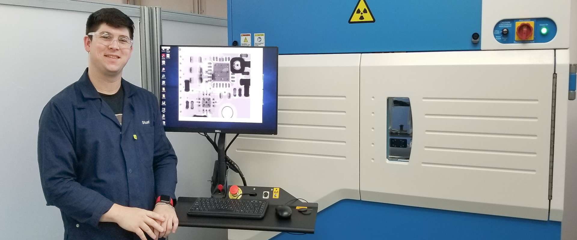
X-Ray Inspection System Components

A typical X-ray inspection system for PCB analysis consists of:
- High voltage X-ray tube source
- Collimator and filters
- Precision manipulator stage
- Scintillator and detector array
- Processing electronics
- Control computer
The core components work together to capture and process X-ray images:
X-Ray Tube – Generates X-rays by accelerating a focused electron beam across a high voltage potential into a metal anode target. This produces a broad spectrum of X-ray wavelengths. Voltages range from 30 to 450 kV based on the penetration required.
Collimator – Focuses the X-rays into a narrow beam directed at the PCB sample. This enhances image sharpness by reducing scatter. Collimator aperture sizes vary from 25 to 500 microns.
Filters – Selective filtration removes lower energy X-rays to tune photon energies for optimum material penetration. Common filters are aluminium, copper, or cerium.
Manipulator Stage – High precision X/Y/Z manipulator stage positions PCB samples within the X-ray chamber. Stages provide positioning accuracy down to 1 micron for sharp imaging.
Detector – A scintillator first converts absorbed X-rays into visible light. Then a sensor array like a CCD or CMOS photodiode matrix captures the emission to generate a grayscale image correlated with X-ray absorption.
Image Processor – Captured images are processed to enhance contrast, subtract background noise, stitch fields of view, and apply analysis algorithms to identify defects.
These components work in concert to produce detailed X-ray visualizations of PCB internals for inspection.
X-Ray Imaging Modes for PCB Inspection
X-ray systems offer various operating modes to optimize detecting different types of defects:
2D Radiography – The simplest imaging mode captures a two-dimensional projected view of the entire PCB from a single angle like a medical X-ray. This reveals defects like missing components, cracked joints, or open vias. But lacks depth information.
3D Tomography – Captures multiple 2D views as the sample is rotated. Software reconstructs these projections into a 3D volumetric model that can be sliced through any axis. Provides complete visualization but at higher inspection time.
2D and 3D Microscopy – Utilizes high magnification microfocus X-ray tubes and finer detector pixels for close inspection of solder joints, wire bonds, and other features. Can produce 2D or 3D views.
Laminography – Slices through at an angle to focus on a plane within the PCB, blurring other regions above and below. This allows inspecting a single board layer in depth without interference.
The imaging mode capabilities match inspection needs whether looking broadly across the entire board or closely examining critical solder joints and interconnects.
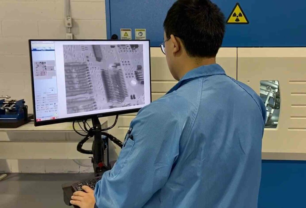
Automated X-Ray Inspection Process

Modern X-ray systems automate and streamline PCB inspection:
- PCBs are loaded into the system manually or by conveyor
- Fiducial markers on the board automatically align imaging fields
- User defines scan areas and parameters through software
- X-ray tube scans over defined regions capturing images
- Images processed to enhance quality and detail
- Algorithms analyze images and highlight potential defects
- Results output with defect locations and classifications
- Operators verify and characterize flagged defects
Automating sample handling, image capture, and analysis minimizes manual work and enhances consistency.
Some systems support inline integration directly into PCB assembly lines. This enables 100% inspection immediately after critical process steps, providing rapid feedback on issues to correct.
X-Ray Inspection Applications
X-ray inspection proves useful at various stages of PCB production and assembly:
Incoming Component Inspection – Scan packaged ICs, connectors, capacitors, and other parts for internal flaws before mounting.
After Solder Paste Printing – Confirm uniform paste application across pads before component placement.
Post Solder Reflow – Verify hidden solder joint quality, solder balling, and open vias under BGAs and QFNs.
Conformal Coating Inspection – Check for coating voids around components vulnerable to environmental contamination.
PCB Stackup Validation – Measure alignment between buried layers and dielectric thickness.
Rework Verification – Inspect repaired solder joints and replaced components.
Failure Analysis – Assist root cause analysis of field failures by viewing internal PCB structure.
X-ray provides a non-destructive window into PCBs that other inspection tools cannot access.
X-Ray Inspection Limitations
While a powerful technique, X-ray inspection does have some inherent limitations to consider:
- Safety – X-ray radiation demands proper system shielding, monitoring, and safety interlocks. Operators require training.
- Image Resolution – Fine pitch components below 0.3-0.5 mm can be difficult to resolve adequately depending on system geometry and settings.
- Light Elements – Low atomic number materials like plastic absorb few X-rays, reducing contrast. Detecting voids or contaminants requires sufficient density differences from surroundings.
- Metal Artifacts – Highly attenuating components like BGA balls obstruct views underneath. Special parallax techniques help minimize this effect.
- Inspection Time – Capturing and processing detailed 3D tomographic images can take minutes per board, limiting throughput.
- Cost – X-ray systems require significant capital investment with prices from $50,000 to $500,000 range.
While not a panacea, X-ray inspection still provides immense utility when used judiciously for targeted process monitoring and defect analysis.
X-Ray vs Optical Inspection Comparison
Optical inspection and X-ray both play important roles in PCB quality assurance:
| Criteria | Optical Inspection | X-Ray Inspection |
|---|---|---|
| Surface Defects | Excellent | Limited |
| Internal Defects | None | Excellent |
| Speed | Very Fast | Moderate |
| Cost | Low | High |
| Image Resolution | 1 micron range | 300+ micron range |
| Color Detection | Yes | No |
| Safety Considerations | Minimal | Significant |
Optical inspection excels at scanning board surfaces rapidly at high resolution. But only X-rays provide internal visibility.
Using both techniques together gives complete coverage:
- Optical inspection provides rapid feedback on assembly quality
- X-ray targets internal defects of concern
This complementary approach maximizes quality while minimizing total inspection burden.
Design Techniques for X-Ray Compatibility
PCBs can be designed to streamline X-ray inspection and enhance defect detection:
- Include fiducials for accurate image alignment
- Allow access to scan critical areas like BGA/QFN pads
- Eliminate unnecessary dense metals that absorb X-rays
- Create “X-ray windows” with clearance cuts in ground planes
- Use round solder mask openings for better joint visibility
- Specify “void-free” interfacing
- Follow design-for-inspection guidelines to avoid tightly packed configurations difficult to image
Simulation tools like Nordson MATRIX exist to model X-ray visibility and optimize designs.
Taking X-ray limitations into account while designing improves inspectability.
Implementing X-Ray Inspection
Follow these general guidelines when implementing X-ray inspection:
- Determine key defect types to detect – missing vias, solder voids, etc.
- Select X-ray imaging mode(s) to best reveal those defects
- Define inspection zones targeting areas of highest concern
- Select X-ray energy levels balancing penetration versus resolution
- Dial-in scan settings for image clarity – filtration, exposures, etc.
- Establish analysis algorithm acceptance criteria based on process capability
- Correlate automated results with manual verification of defects
- Capture metrics to fine tune process window and control limits
As with any process monitoring, the effectiveness depends on mindfully gathering and assessing results to hone defect detection fidelity and yields.
Conclusion

X-ray imaging enables powerful internal inspection of PCB assemblies to reveal defects undetectable through optical means. Advantages like solder joint metrology, failure analysis assistance, and process control feedback make investing in X-ray systems worthwhile for many electronics manufacturers.
As component densification marches on, X-rays provide unique quality assurance visibility. Yet awareness of limitations is important to apply the technology judiciously where it provides maximal benefit. Combined with optical inspection, X-rays offer electronics producers extensive real-time quantitative defect data to improve manufacturing lines and ensure the highest quality and reliability standards.
Frequently Asked Questions
What types of defects can X-ray inspection best detect?
X-ray imaging excels at finding voids in solder joints under components, viewing inner layer misregistration and dielectric thickness, scanning for missing vias/pads, and validating proper paste deposition.
Does every PCB manufacturer need X-ray inspection?
Not necessarily. Optical inspection meets basic QA needs for many. But X-ray becomes advantageous for mission-critical boards with high component densities or hidden interconnects requiring quality validation.
What X-ray safety standards apply to PCB inspection systems?
Equipment must comply with radiation safety regulations and containment requirements. For the US this includes CDRH/FDA standards. Operators require proper X-ray training.
Can X-ray damage the PCBs or components being inspected?
In general the low X-ray doses used cause no component or board degradation. But radiation hardening may be needed for highly sensitive electronics.
What is the typical resolution achievable with PCB X-ray systems?
1-2 mil resolution is possible for microfocus 2D imaging. 3D computed tomography typically achieves 3-5 mil resolution due to geometric blurring. Finer features become difficult to adequately resolve.


