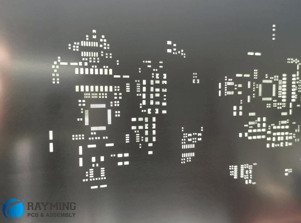
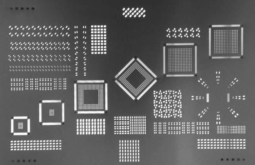
Printed circuit board (PCB) stencils comprise thin metal sheets containing cutouts used for applying solder paste onto pads during surface mount assembly. Stainless steel offers an ideal stencil material given durability, chemical resistance and ease of cleaning necessary for repeat usage over PCB production runs.
Various methods exist for manufacturing stainless steel stencils including laser cutting, chemical etching and electroforming. This guide examines stainless steel stencil properties, design considerations, production approaches, usage tips and storage precautions necessary for handling these critical SMT consumables determining first-pass soldering success.
Overview of Solder Paste Stencils
Solder paste stencils help accurately deposit paste:
Solder Paste – Flux vehicles carry tiny solder balls
Stencil Apertures – Print precise amount onto pads
Rolling Squeegee – Shears off paste imprinting PCB
This rapid additive solder deposition process facilitates bulk lead-free solder alloy attachment across copper pads ultimately securing surface mount device (SMD) components onto boards following curing and reflow stages ensuring both mechanical and electrical connections vital for subsequent functioning during product lifetimes.
Need for Stainless Steel Stencils

Stainless steel crafts premium stencils given:
Durability – Harder than brass withstanding repeated high temperature soldering without softening microscopic aperture features risking degradation losing initial dimensional accuracy necessary for sustaining precise paste deposits matching various land patterns.
Dimensional Stability – Low coefficient of thermal expansion retains original size without substantial contraction/expansion across temperature swings experienced intermittently when printing boards during daily production shifts.
Chemical Resistance – Withstands corrosive organic acids within solder paste and cleaning solvents preventing premature breakdown or warp aiding longevity over numerous printing cycles further amortizing costs.
Reusability – Repeated cleaning allows stainless steel stencil reuse over long durations making up for higher initial material expenses through extended utility lifespan during programs production runs minimize expenses from frequent stencil consumable replacements.
Ease of Inspection – Reflective sheen assists microscopic visual scrutiny finding subtle debris clogs or scratches around openings impacting paste transfer.
Thereby stainless steel material properties greatly benefit stencil functionality during solder paste imprinting processes making invaluable components across electronics surface mount workflows.
Key Stencil Terminology
Important stencil parameters include:
Material Thickness – Determines minimum aperture sizes, durability, paste release
Print Side Wall Angle – Sharp edges assist paste release while angled walls fine tune deposits
Aperture Opening Size – Match site pad dimensions, compensate for tolerances
Border Openings – Aid scraping excess paste preventing outside smearing
Fiducials Marks – Assist identical alignments onto PCBs for accurate prints
Underside Etching – Lowers contact area with PCB avoiding trapped paste
Getting these right ensures good solder joints later.
Design Considerations for High Quality Stencils
Various factors influence stencil design:
PCB Land Patterns – Match aperture sizes to pads with compensation for registration errors
Paste Volume Targets – Sufficient material needing clean pick and place release
Alloy Particle Size – Type 3 or 4 matching standard/fine pitch paste preventing clogging
Aperture Wall Angle – Typically between 60-75° balances paste release
Border Openings – Around 20% larger than typical pads ease scraping without bridges
Fiducing Marks – Numerous fiducials on both sides confirming alignments
Underside Etch – Lowers stencil undersurface area trapping paste
Rounded Corners – Prevent paste smear into gap between sharp print board interface corners
Getting appropriate geometries necessitates checking fabricated stencils against original datasheets confirming compliance verifying reliable performance.
Laser Cut Steel Stencil Production
Laser machining cuts complex stainless steel stencils accurately:
Step 1 – Design File Preparation
- Import customer Gerber and assembly prints
- Check design rules on minimum aperture sizes etc
- Compensate pad dimensions allowing alignment margins
- Add reference fiducial marks
- Specify aperture wall angle, corner style etc
This readies the drawing for machining.
Step 2 – Material Selection
- Choose steel thickness balancing durability versus flextural rigidity
- Consider effects of material finishes or coatings on fine features
Proper thickness minimizes aperture deformations during usage.
Step 3 – Laser System Programming
- Import stencil patterns into laser machining software
- Set cutting areas, speeds, aperture styles etc
- Define tool paths optimizing cycle times
- Insert probe points checking cut quality
This automation maximizes cutting accuracy.
Step 4 – Stainless Steel Machining
- Secure steel sheet onto cutting bed
- Progressively cut apertures using ultraviolet pulsed laser
- Periodically validate quality against criterias
- Exercise precision hole drilling forming fiducials
Watchfully monitor ongoing dimensions during gradual area-by-area machining.
Step 5 – Post Processing
- Microscopically inspect aperture quality
- Gentle brush clean surface debris avoiding scratches
- Pack between stiffeners preventing bend damage
Thorough cleaning readies stencil for solder paste printing usage.
Chemical Etch Stencil Fabrication
Chemical etching also generates steel stencils reliably:
Step 1 – Photoresist Application
- Thoroughly clean and dry stainless sheet
- Apply liquid Epoxy or dry film photoresist layer
- Soft bake evaporating solvents hardening resist
This prepares blank canvas for imaging.
Step 2 – Mask Imaging
- Print aperture patterns onto transparencies
- Align film onto steel for exposure consistency
- Cure specific areas using high intensity UV
Aperture shapes get printed onto steel sheet.
Step 3 – Chemical Developing
- Developer solution dissolves UV exposed regions
- Stop bath arrests developing preventing undercuts
- Rinse off remaining resist residues
This reveals open areas eventually becoming stencil apertures.
Step 4 – Controlled Etching
- Immerse sheets into iron chloride etchant bath
- Agitate containers allowing fresh reagent contact
- Drain, rinse and dry sheets after timed depth cuts
Chemical dissolution carves out apertures through stainless sheets.
Step 5 – Photoresist Stripping
- Soak fully etched sheets into resist stripper bath
- Use bristle brushes removing stubborn polymers
- Thoroughly rinse and dry stencils
This fully reveals finished apertures ready for solder paste printing.
Key Attributes of Premium Steel Stencils
High performance stencils boast excellent:
Resolution – Mesh count reaching 0.001” lines resembling fine window screens
Positional Accuracy – Tight fiducial marks assist precise alignments
Plate Flatness – Limit 0.002”/inch twist over large areas
Aperture Consistency – Uniform side-wall angles; clean edges
Surface Finish – Low average roughness avoiding paste sticking
Laser Etch Resistance – Withstand repeated cleanings without distorting
Material Certification – Validation for ROHS lead-free compliance
Careful attention across above parameters satisfies discerning SMT production environments minimizing yield detractors.
Specialized Stencil Technologies
Advanced stencils meet niche requirements:
Zero-Slump Stencils – Thick apertures preventing paste ooze
Foil-Framed Stencils – Metal surrounds reinforcing stability
Nano-Coated – Non-stick layers improve paste release
Dual Thickness – Mix thick and thin areas fine tuning deposits
Electropolished – Smooth microscopic finish further aids release
Aluminum Base – Lightweight material handles large boards
Such options balance durability against precision tailoring performance for challenging assemblies needing exact paste metering across irregular boards containing regions needing fine pitch tolerances interspersed among standard spaces allowing programmatic mixing-matching customized regional attributes amalgamating strengths from standalone offerings unavailable hitherto through unified composites.
Solder Paste Printing Using Steel Stencils
Follow these procedures when applying paste using steel stencils onto PCBs:
Phase 1 – Stencil Cleaning:
- Gently wipe down stencil surface with isopropyl
alcohol avoiding excess contact pressure - Ensure stencil properly dries afterwards
This prepares clean canvas for next application.
Phase 2 – Stencil Mounting:
- Carefully align stencil fiducials onto respective PCB
- Use fixture pins temporarily stabilizing placement
Accurate alignments prevent smearing issues later.
Phase 3 – Solder Dispensing:
- Slowly roll narrow bead over stencil area using press bottle
- Gradually flood entire PCB surface with paste
- Avoid excess paste along printing sidewalls
This distributes paste across stencil interior areas.
Phase 4 – Print Stroking:
- Firmly hold PCB against vacuum table if available
- Unidirectionally sweep soft rubber squeegee blade across paste
- Apply 5kg consistent pressure for clean scrape
Shearing action presses paste through apertures onto pads below.
Phase 5 – Stencil Separation:
- Carefully lift stencil away from populated board
- Inspect paste deposits and land coverage quality
- Realign and reprint if necessary
This check prevents first-pass yield issues.
Phase 6 – After-print Cleaning:
- Wipe underside using non-abrasive lint-free swab
- Gently brush clean paste residues inside apertures
- Store stencil only after ensuring completely dry
Proper maintenance maximizes stencil lifetimes.
Optimizing Aperture Fills

Even seasoned operators require initial print tuning when working new designs:
Insufficient Printing – Enlarge stencil openings allowing more paste filling land areas
Overprinting – Shrink apertures decreasing paste volumes to avoid bridges
Smears or Skips – Adjust blade pressures, paste viscosity properties
Fine tuning maximizes first pass yield keeping defects within acceptable levels needed for economical SMT line operation devoid of expensive rework or touchup. Statistical trending during such empirical optimization provides operational feedback guiding eventual modifications reaching stable processing criteria satisfying objectives.
Stencil Maintenance Best Practices
Proper stencil care ensures consistent printing quality:
- Inspect aperture quality before/after each usage
- Establish stencil life tracking system logging prints
- Follow recommended cleaning cycles
- Avoid excessive wiping, brushing or ultrasonic intensity
- Store horizontally suspended within framed enclosures
Implementing robust maintenance protocols improves fab process stability necessary for uninterrupted production flows vital reaching volume electronics reliable delivery targets crucially important sustaining customer trust through consistent defect free outputs even surmounting hidden obstacles before manifestation by investing during incremental improvements steps continually elevating baseline benchmarks standards.
Stencil Storage Precautions
Storing stencils improperly risks damage shortening utility lifespan:
- Dents – Avoid contact with harder objects indentation prints
- Warp – Improper folder tension may distort flatness
- Chemical Exposure – Solve spillage degrading laser cuts
- Aperture Clogs – Dust particle embedding hampers paste transfer
- Oxidative Corrosion – Humid air forms surface stains without controlled humidity storage
Thereby keeping apt enclosures prolongs stencil serviceability over numerous iterative PCB prototyping or volume production activities before necessitating replacements.
Conclusion – Importance of Premium Steel Stencils
Stainless steel stencils play indispensable roles rapidly imprinting solder pastes on increasingly diminutive surface mount pads driving electronics miniaturization. Hence procuring appropriately thick steel sheets from qualified suppliers complemented using proven laser machining, chemical etch patterning and meticulous maintenance best practices sustains reliable first pass deposition yields bottlenecking overall operational productivity metrics eventually manifesting end-product quality once subjected solder reflow furnaces transforming discrete paste bricks into robust intermetallic joints eventually empowering functional boards. Technology improvements on pastes, complemented by continual stencil material and patterning innovations addressing escalating density assembly challenges confronts electronics packing densities scaling limitations by progressively pushing fabrication boundaries through synergistic chemical-mechanical advances jointly navigating uncharted domains reaching newer milestones.
Frequently Asked Questions
What thickness steel works best for SMD stencils?
For most SMT assembly applications with SAC305 lead-free solder, stencil thickness ranging between 4 to 6 mils offers the optimum balance WRT minimum aperture resolution, print durability, paste release and flextural stresses preventing template warping during usage thereby ensuring reliable imprint replication uniformity imperative for target paste deposition across myriad device pads prior to component placement minimizing latent first pass solder join defects.
What aperture shapes fine tune paste printing?
Common aperture shape adaptations fine tuning paste volumes include rounded/beveled corners preventing excess material accumulation building up at pattern extremities known causing intermittent bridge shorts. Moreover adjust aperture land width ratios between 60% to 80% relatively pads diameters together with judiciously wall angles maximize process windows hitting print yield sweet spots.
How are stencil and pad misalignment handled?
Acceptable SMD stencil alignment tolerance budgets typically span under +/-10mils relative PCB pads centers. Rectifying separation distances expected from fabrication and assembly shop registration capabilities demands appropriately biasing nominal aperture dimensions beforehand through compensation swelling or shrinkage for pastoral total transfer capacities inside increased routed destination territories counterbalancing anticipated mechanical positioning deviations incurred at various steps.
When do stencils require replacing?
Sustaining adequate solder paste deposit repeatability during production requires replacing stencils approximately around 150-400 print cycles depending on thickness. 5 mil stencils approach end-of-life faster than sturdier 10 mil versions. Production engineers track defects, undersized prints or smearing clips formally assessing diminishing stencil utility justifying asset retirement and replacements restoring fabrication yields.
How do you store solder paste stencils?
Controlled environment storage using vacuum sealed moisture barrier bags containing desiccant packs proves essential for longevity high quality laser cut or chemical etched stainless steel SMT stencils avoiding oxidation or chemical ingress degrading fine aperture features from acidic paste fluxes ultimately impacting paste transfer efficiency causing operational yields whenever degraded tools reutilization refrain otherwise necessitating premature expensive consumables replacement draining expenses deteriorating profit margins.


