Printed wiring boards (PWBs) and printed circuit boards (PCBs) are crucial components of electronic devices and equipment. From computers and smartphones to industrial machinery, automotive systems and advanced medical devices, PWBs and PCBs provide the foundations for electronics and connectivity.
But what exactly distinguishes PWBs from PCBs? At a glance the terms seem interchangeable, yet there are subtle differences. This article will dive into PWB and PCB specifics to highlight the key similarities and differences in terminology, materials, manufacturing processes and applications.
We’ll overview:
- Defining attributes of PWBs and PCBs
- Composition and constituent elements
- Fabrication techniques
- Quality testing procedures
- Use cases and applications
Grasping PWB vs PCB distinctions aids engineers, designers and manufacturers when conceptualizing and actualising electronic device internals. Let’s compare.
Key Characteristics of PWBs and PCBs
What is a Printed Wiring Board (PWB)?
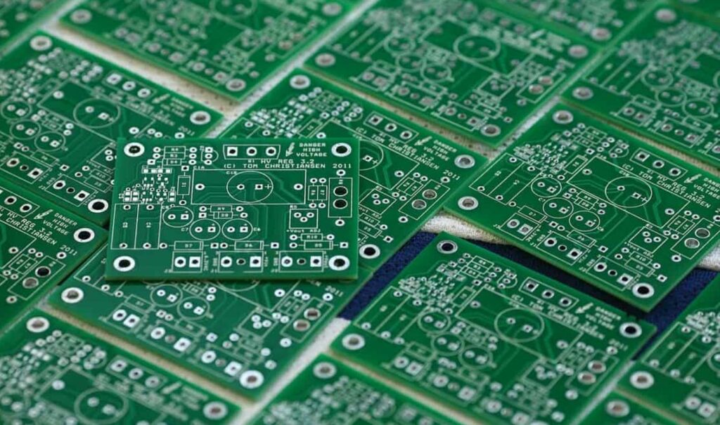
A printed wiring board refers to the bare circuit board containing only:
- Substrate material (like FR-4 fiberglass)
- Patterned copper traces and pads
- Plated through holes and vias connecting layers
The PWB forms an interconnected matrix allowing installation of components. They provide mechanical structure and electrical links without active devices or components prior to population.
What is a Printed Circuit Board (PCB)?
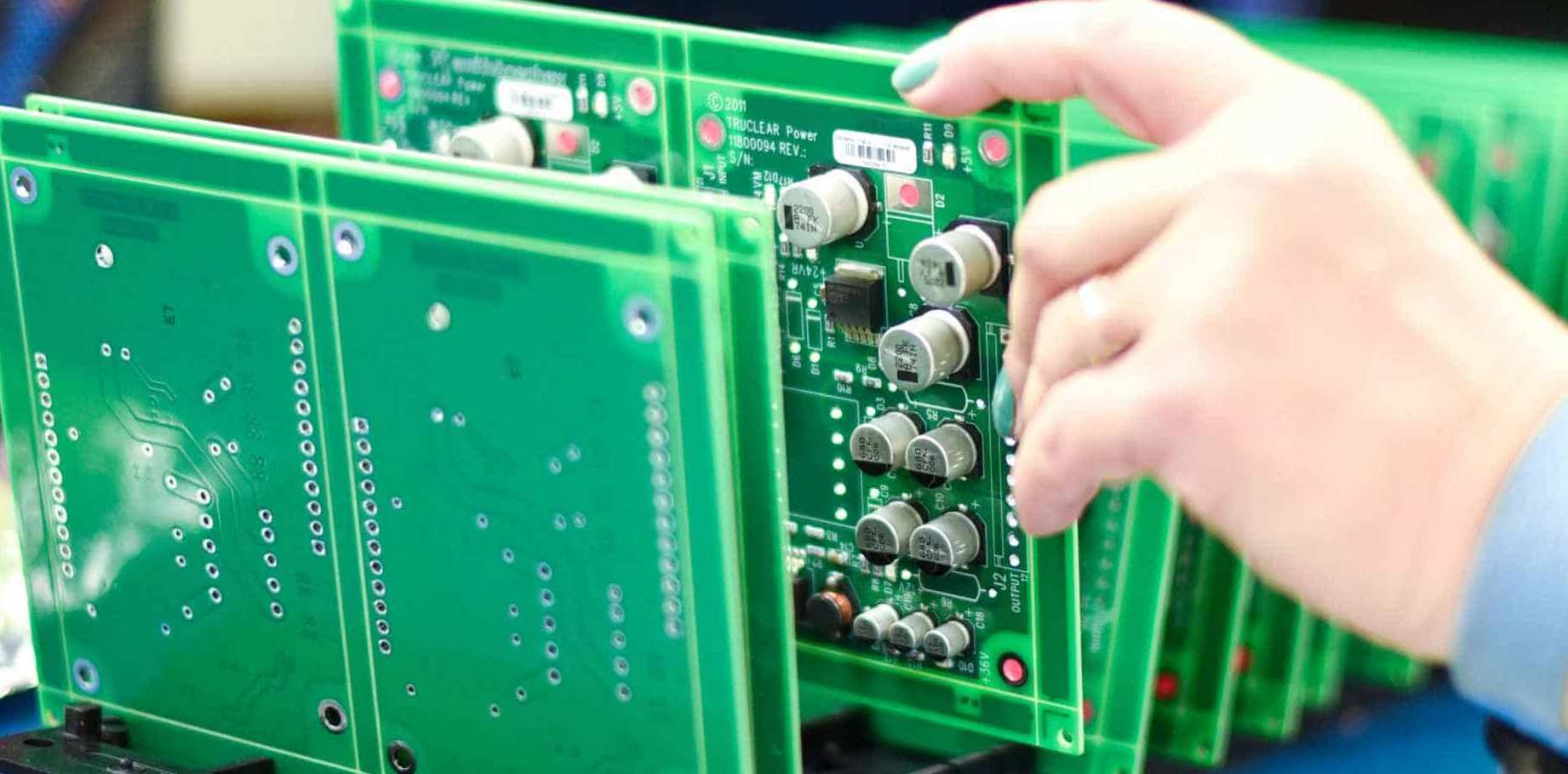
A completed populated printed circuit board contains both passive and active components attached to the base wiring board. This includes resistors, capacitors, integrated circuits (ICs), processors, connectors and other parts that enable functionality.
So while often used interchangeably:
- PWB refers specifically to unpopulated board
- PCB indicates fully assembled board
Subtle differentiation, but important as we explore fabrication and design considerations that differ between the two in stages of production.
PWB and PCB Composition Comparison
Both entities share common fundamental elements and materials as outlined below:
Substrate Materials
This forms the foundational layer boards are constructed upon. Typically thermoset laminates that are rigid and non-conductive, including:
- FR-4: Woven fiberglass cloth with an epoxy resin binder
- CEM-1, FR-2: Paper fabric laminates (less common nowadays)
- Ceramics, polyimides: For high temperature, flexibility needs
Conductive Copper Traces
Etched or printed copper traces define wiring transmission paths allowing electric signals to propagate between points. Multiple conductive layers stack up forming wiring networks.
Dielectric Layers
Interleaved non-conductive dielectric layers provide insulation between copper layers, preventing short circuits while allowing layered signal routing.
Common dielectrics:
- FR-4 Prepreg
- Polyimides
- Epoxy blends
- Ceramic filled composites
Fabrication Processes
PWBs and PCBs leverage many of the same fundamental fabrication techniques, albeit with some divergence in specific methods between stages from bare boards onwards as population requires adaptations.
Shared Initial PWB Processing
- Substrate Material Laminating: Base insulating substrate layer creation via laminating glass fabric and resin
- Conductive Layer Addition: Copper foil layer bonding
- Etching: Photolithographic masking and chemical etching to form circuit trace patterns from copper layers
- Hole Drilling: Drill through holes and vias for electrical interconnections including plating
- Outer Layer Imaging: Additional photolithographic patterning of outer copper layers
- Surface Finishes: ENIG, immersion silver, HASL, reflowed tin finishes applied to protect exposed copper traces
These initial PWB processing steps establish conductive trace networks across layered PWB substrate prior to components being installed should it become a populated / functional PCB.
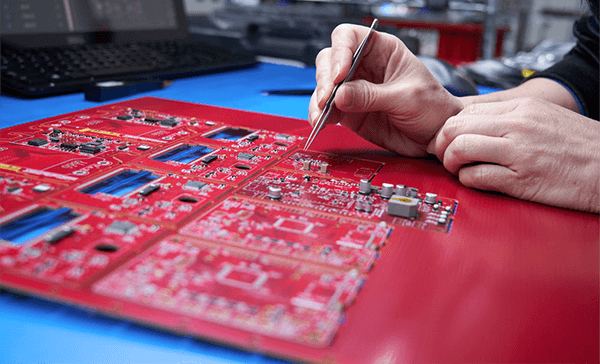
Further PCB Assembly and Population
Printed circuit boards diverge from this point onwards with active and passive components installed to impart functionality:
- Solder Paste Application: Prepare conductive adhesive paste regions
- Pick and Place: Robotic component installation
- Reflow Soldering: Heat profile to reflow solder paste binding components
- Additional Processes: Potting resins, protective coatings, etc.
- Conformal Coating: Optional protective material overcoat layer
- Programming: Flashing firmware onto programmable devices
The PCB population transforms base PWB into a functional circuit board able to perform intended tasks.
Key Fabrication Differences
| PWB | PCB |
|---|---|
| Bare substrate board | Substrate + components |
| Just conductive traces | Active devices, passives etc. added |
| Younger technology | Additional fabrication steps |
| Lower initial cost | Increased cost from population |
| Simpler processing | Complex population processes |
So while sharing common early fabrication stages, PCBs require considerable additional manufacturing steps to mount and interconnect electronic components needed for functionality.
Testing Methodologies
Verifying board integrity at various production stages is crucial before deployment. Let’s explore key testing procedures:
PWB Testing
Assessing base boards involves checkpoints like:
- Dimensional conformity checks
- Visual layer alignment checks
- Impedance testing matched to characteristic impedance target
- Interlayer connectivity testing on all drilled holes/vias
- Confirming effective copper thickness, hole plating
- Adhesion pull off testing preventing delamination
This establishes whether conductive pathways are laid out correctly prior to active devices being fitted during PCB population.
PCB Testing
Populated boards require not just electrical but functional validation:
- Net connectivity validation
- Ground continuity verification
- Board interfacing and communication bus correctness
- Power sequencing during startup/shutdown
- Functionality checking each peripheral works
- Confirming fault tolerance ability
- Stress testing borderline voltage/temp/frequency thresholds
Thorough PCB testing across operating state space ensures populated boards operate reliably as system components.
Applications and Use Cases
Printed wiring boards and populated printed circuit boards share extensive use cases across electronics:
Common Applications
- Computers: Motherboards, graphics cards, SSDs
- Home/Office Devices: Routers, printers, appliances, power tools
- Consumer Electronics: Phones, wearables, smart home tech
- Automotive: Engine control units, dashboards, infotainment
- Industrial: PLCs, process controllers, robotics systems
- Medical: Diagnostic systems, dental, surgical devices
- Military/Aerospace Avionics: Aircraft onboard systems, missiles
- Research: Prototyping boards, custom instrumentation
Unique PCB Specializations
Certain application spaces utilize highly specialized printed circuit boards:
High Speed Digital
- High density interconnects
- Tight impedance control
- Low cross-talk
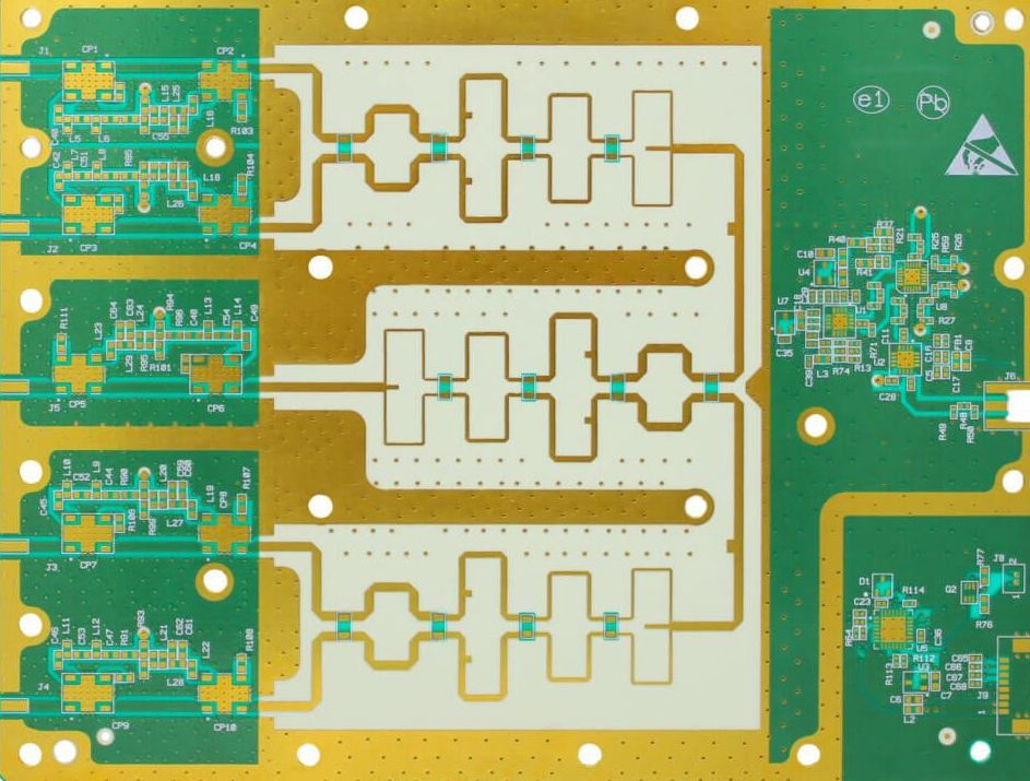
High Frequency RF
- Tight dielectric tolerances
- Controlled laminate transitions
- Buried & blind vias
- Mixed signal
High Power
- Thermal management
- Large copper sizes
- Ceramic substrates
- SnPb finishes
So while sharing broad use cases, PCBs tailor and optimize fabrication for specific application constraints.
PWB vs PCB Comparison Summary
| Metric | PWB | PCB |
|---|---|---|
| Definition | Bare wiring board | Populated functional board |
| Composition | Substrate, wiring | Components mounted to PWB |
| Fab. Processes | Imaging, etching, drilling | Additional assembly, placement, soldering, programming |
| Testing | Structuralintegrity, connections | Plus functional validation |
| Use Cases | Precursor to PCB | Broader deployment after population |
This covers the key differences. While incomplete boards in isolation, PWBs constitute first base “half” of final PCB units.
Frequently Asked Questions
Still hungry for more PWB versus PCB details? Below are common FAQs.
FAQ #1: Are PWB and PCB the same thing?
Not quite. As outlined, PWB refers specifically to the bare wiring board prior to components being installed. PCB indicates fully populated boards. They share early fabrication but PCB has additional processing.
FAQ #2: Can you have a PCB without a PWB?
No, all PCBs require a precursor PWB to form the underlying physical wiring infrastructure to mount components onto. The PWB allows routing signals between populated electronic devices.
FAQ #3: What came first, PWB or PCB?
Printed wiring boards technology slightly preceded the advent of printed circuit board assembly and population processes. So PWB at a simpler initial stage of development.
FAQ #4: Can a PWB function like a PCB?
No. While providing structured physical layers and connectivity, a PWB has no active or passive electronic components so cannot perform computation, power delivery or other functions required of a PCB.
FAQ #5: Are PWBs cheaper or more expensive than PCBs?
PWBs are cheaper at their earlier stage since they involve fewer fabrication steps compared to populated PCBs which require full assembly. But pricing varies drastically based on complexity, volume and other factors.
Conclusion
We’ve illuminated printed wiring boards constitute an intermediary foundation enabling progression to functional printed circuit boards. PWBs establish essential interconnect infrastructure populated boards are then assembled upon using additional fabrication techniques.
PWBs introduce early physical wiring matrices while PCBs realize fully fledged electrically functional assemblies for diverse electronics applications. These concepts aid technical understanding for engineers and manufacturers when visualizing, planning and producing electronic systems of escalating complexity.
Whether dealing with simple internal wiring or cutting edge populated multilayer boards enabling bleeding edge applications, printed wiring board and printed circuit board foundations remain universal across modern electronics. This exploration has shed light explaining their crucial symbiotic relationship.


