Introduction to Plated Through Holes (PTHs)
Plated through holes (PTHs) are conductive holes extending vertically to interconnect all layers in multilayer printed circuit boards (PCBs). Metallic conductive walls coat the through holes with pads at both ends.
PTHs enable:
- Vertical connectivity linking all PCB layers
- Component lead and solder fillet connectivity
- Passing high currents between layers
- Improved reliability over non-plated holes
Understanding PTHs – how they’re constructed, key properties, design factors, application impacts and tradeoffs – aids PCB design and manufacturing for optimized functional boards.
In this article we’ll explore common PTH questions covering:
- The fabrication process
- PTH attributes and parameters
- Structures and variations
- Reliability factors
- Design and manufacturing considerations
- Functionality impacts
Equipped with comprehensive PTH insights you’ll be able to enhance next-generation PCBs. Let’s get better acquainted with these crucial vertical interconnect conduits.
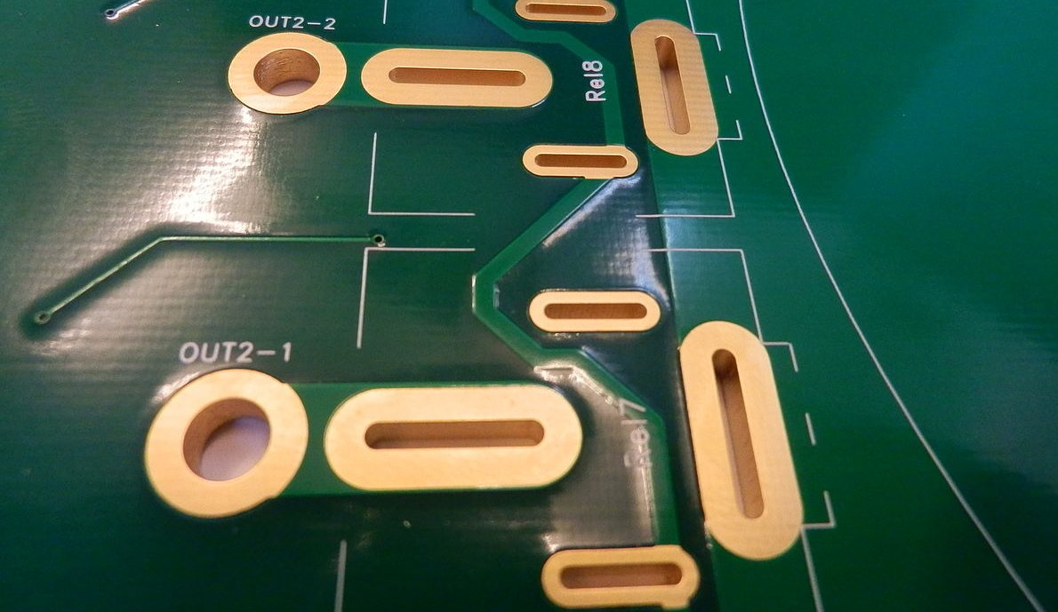
Anatomy of a Plated Through Hole
PTHs comprise round holes extending fully through the PCB substrate coated by a conductive metal layer. This creates hollow electrically continuous pathways through the board:
Key characteristics:
- Holes mechanically drilled through PCB layers
- Conductive metal plating lining hole walls
- Connecting pads on top and bottom surfaces
- Allows interlayer connectivity of components
The plated metal barrel electrically connects all internal and external conductive layers in one continuous link enabling signals to pass vertically across the entire PCB stackup unimpeded.
Next let’s overview the step-by-step PTH fabrication sequence during PCB production.
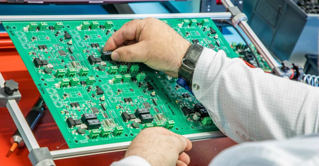
How Plated Through Holes are Made
PTHs get fabricated into boards during multilayer PCB manufacturing through sequential precision processes:
- Drilling – Holes mechanically drilled through substrate
- Deburring – Remove rough edges around holes
- Etching – Desmear epoxy resin smear
- Seed Layer – Sputter thin copper film layer
- Electroplating – Electrically deposit copper thicker coating
- Outer Layer Connection – Join plating to signal layers
This achieves hollow copper walled channels through the entire board ready for component connectors.
Understanding the fabrication sequence enables appropriate PTH specification targeted to final application, manufacturing capabilities and end product lifecycle demands.
Now let’s shift to examining key attributes and parameters defining PTHs for design.
PTH Attributes and Characteristics
PTHs are primarily defined by physical dimensions, plating construction, spacing and drilling precision capabilities:
| Attribute | Typical Range | Definition |
|---|---|---|
| Aspect Ratio | 2:1 to 15:1+ | Ratio of thickness (z height) to diameter |
| Diameter | 0.15mm to 0.89mm | Widest internal width size |
| Plating Thickness | 25μm to 76μm | Inside conductive metal layer depth |
| Pad Diameter | 130% to 250% of hole size | Surface connection size |
| Accuracy | ±0.05mm | Allowable deviation of hole position |
| Pitch | 2 to 4 hole diameters | Adjacent hole spacing distance |
Note: imperial units also commonly used (mils)
Additionally important PTH figures of merit:
- Current rating – 20A per hole typical
- Resistance – < 0.015 Ω typical
- Impedance – Characteristic impedance ~50Ω (can be engineered)
Observing fabrication tolerances and design rules checking (DRC) during layout requires cross-checking these interdependent PTH characteristics for manufacturability and performance.
Now we’ll discuss common plating structures and PTH elements.
PTH Constructions and Variants
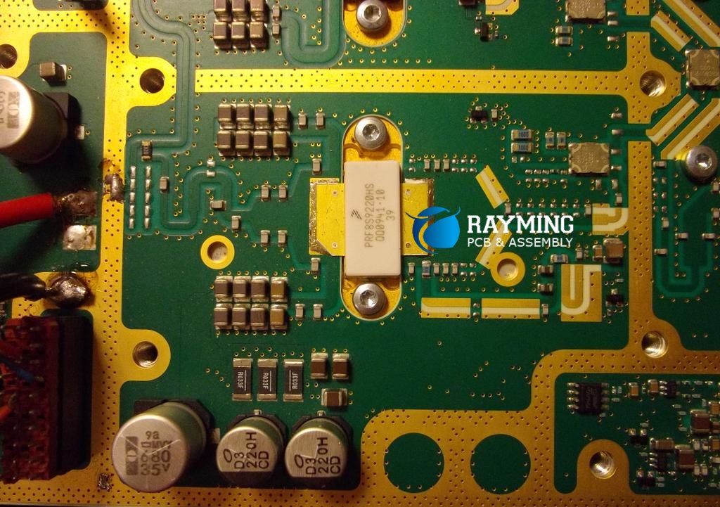
Modern interconnect requirements impose complex demands on plated through holes driving numerous adaptations:
Simple Straight PTH
The conventional straight uniform diameter copper barrel. Simpler but can cause lamination voids.
Back-Drilled Hole
Partial inner substrate hollowed removing laminate. Lowers capacitance but harder to fabricate.
Extended Land
Enlarged connection pads boost component lead reliability. Eases mounting tolerances.
Further variants exist:
- Blind/Buried – Don’t pass fully through PCB layer stackups
- Filled/Capped – Entirely or partially filled with epoxy resin
- Stepped – Switched diameters via precision drilling
The vast range of application-specific plating geometries provides extensive flexibility. Optimized PTHs boost reliability, packaging density, routing capacity and electrical flow.
Next we’ll consider the factors influencing PTH robustness and lifespan.
What Affects PTH Reliability?
Plated through holes act as “vertical wiring channels” through PCBs. Their sturdiness ensures overall product reliability across decades of thermal/mechanical stresses:
Reliability challenges:
- Cratering – Pad lifting around barrel
- Separation – Inner wall delamination
- Wicking – Copper dissolving along glass fiber
- Corrosion – Oxidation degrading walls
Enhancing longevity requires:
- Pairing compatible PCB materials
- Eliminating contaminant residues
- Optimizing fabrication process stability
- Thermal cycling assurance
- Outer pad interface optimization
When factoring reliability, striking a balance between idealized plating procedures and manufacturable processing with acceptable defects is key. Even minor process deviations can incubate failure precursors.
Next we’ll consider the design and fabrication ramifications of PTHs.
PTH Design and Manufacturing Considerations
Incorporating plated through holes influences physical, electrical and production factors:
| Consideration | Ramifications | Mitigations |
|---|---|---|
| Via Tenting | Masking over hole can cause opens | Clearance around pads |
| Spacing | Tight spacing limits capture pad size | Allow 2x hole spacing |
| Capturing | Inadequate annular ring risks disconnect | 0.2mm pad clearance |
| Stubborn Drill | Exit breakout causes tearing | Entry/exit glass style |
| Barrel Crack | Plating separation blocks conduction | Low temp cycling, reduce thickness |
| Registration | Layer misalignments hamper yield | {150-200}μm tolerance budget |
Engineers balancing dense packaging against reliable assembly yield require awareness of these PTH subtleties which impact design, review and production.
Furthermore, fabricators handle PTHs during sequential buildup focusing on productivity versus precision:
| Process | Priority | Impact |
|---|---|---|
| Drilling | Speed | Hole accuracy & HAZ |
| Plating | Thickness | Deposit roughness & ductility |
| Etching | Rate | Undercut risk |
| Outer Layers | Alignment | Minimize registration offsets |
| Testing | Functional | Detect micro-defect precursors |
Asking probing questions when engaging board shops on capabilities, acceptable tolerances, failure analysis and process nuances prevents unwelcome surprises.
Now having covered the elements defining plated through holes, let’s examine how they influence final PCB functionality when deployed.
PTH Functionality Impact
Beyond physically connecting printed circuit board layers, PTHs affect surrounding electrical parameters and behaviors:
Electrical conductivity
- Channels signals vertically
- Reduces conduction losses
- Microwave/RF performance
Electrical isolation
- Can radiate signals inducing cross-talk
- Excessive density or proximity risks shorts
Thermal dissipation
- Heat flow conduit between layers
- Copper & plating act as heatsinks
- Impacts component cooling
EMI shielding
- Plating continuity blocks emissions
- Stitched boundary vias form Faraday cages
Mechanical anchoring
- Component leads resist shear forces
- Reinforces physical board strength
Often overlooked functionality considerations should inform PTH inclusion, location and layout during design stages rather than late or retrospective fixes.
With PTH non-ideality unavoidable at scale, let’s now cover common PTH queries.
Frequently Asked PTH Questions
Q: Can you solder through holes without plating?
A bare PCB hole lacks metallization so won’t wet effectively with solder. Partial unreliable connections likely. Always plate holes intended for component termination.
Q: What size wire fits in a 0.6mm PTH?
As rough guideline, 20AWG wire may fit 0.6mm holes, but given plating thickness budget at least 18% larger. Heat stress and wire insulation will further reduce capacity.
Q: Can PTH cracking cause electrical failure?
Absolutely. Cracks along the interior plating barrel insulate the signal path. Further environmental contamination then accelerates localized corrosion eventually inducing complete PTH failure.
Q: How many vias should a BGA pad have?
Ideally each BGA pad would feature 4 supporting corner PTH vias. However this density proves extremely difficult to manufacture reliably, so engineering tradeoff decisions around via quantity, proximity and layout are necessary.
Q: Can PTH failure cause problems apart from the hole?
Failure precursors like microfactures or subsurface contamination essentially seed defects that over lifetime propagate outwards potentially undermining surrounding laminate or interfaces, leading to secondary solder joint or pad lifted failures.
Conclusion
We’ve thoroughly overviewed printed circuit board plated through holes including fabrication, reliability factors, functionality impacts and design tradeoffs demonstrating their indispensable role interconnecting modern electronics both physically and electrically at microscopic scales.
PTHs contract yesterday’s hand wired boards into tomorrow’s multilayer assemblies. Flush summits enable packing billions of transistor gates under BGA packages. Smooth copper barrels channel GHz data rates vertically through electrically quiet layer planes effortlessly.
Leveraging plated through hole technology with expert proficiency ultimately supports transformative high speed, high complexity and high reliability product breakthroughs changing the world one micro-conduction channel at a time.


