Introduction
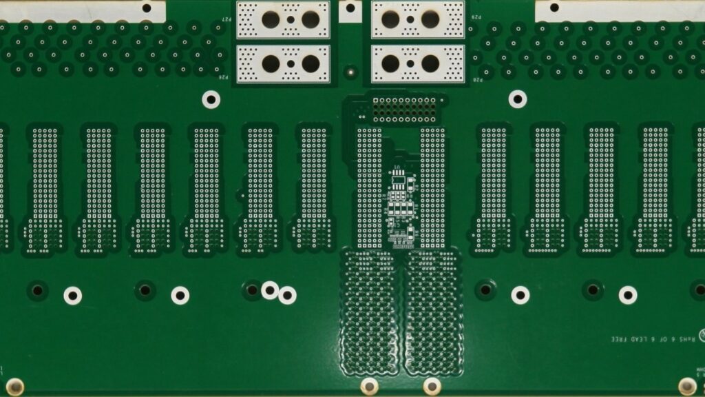
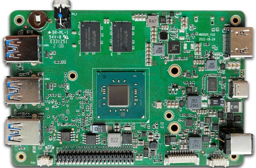
Printed Circuit Boards (PCBs) are essential components in the electronics industry, serving as the backbone for various electronic devices. These boards are composed of various materials, each playing a crucial role in ensuring the proper functioning and reliability of the circuit. In this comprehensive article, we will delve into the world of PCB materials, exploring their properties, applications, and the factors that influence their selection.
What are PCB Materials?
PCB materials refer to the different substances and compounds used in the construction of printed circuit boards. These materials can be broadly categorized into the following categories:
- Substrates: The base material upon which the conductive layers and other components are mounted. Common substrate materials include:
- FR-4 (Flame Retardant 4)
- CEM (Composite Epoxy Material)
- Polyimide
- Aluminum
- Ceramic
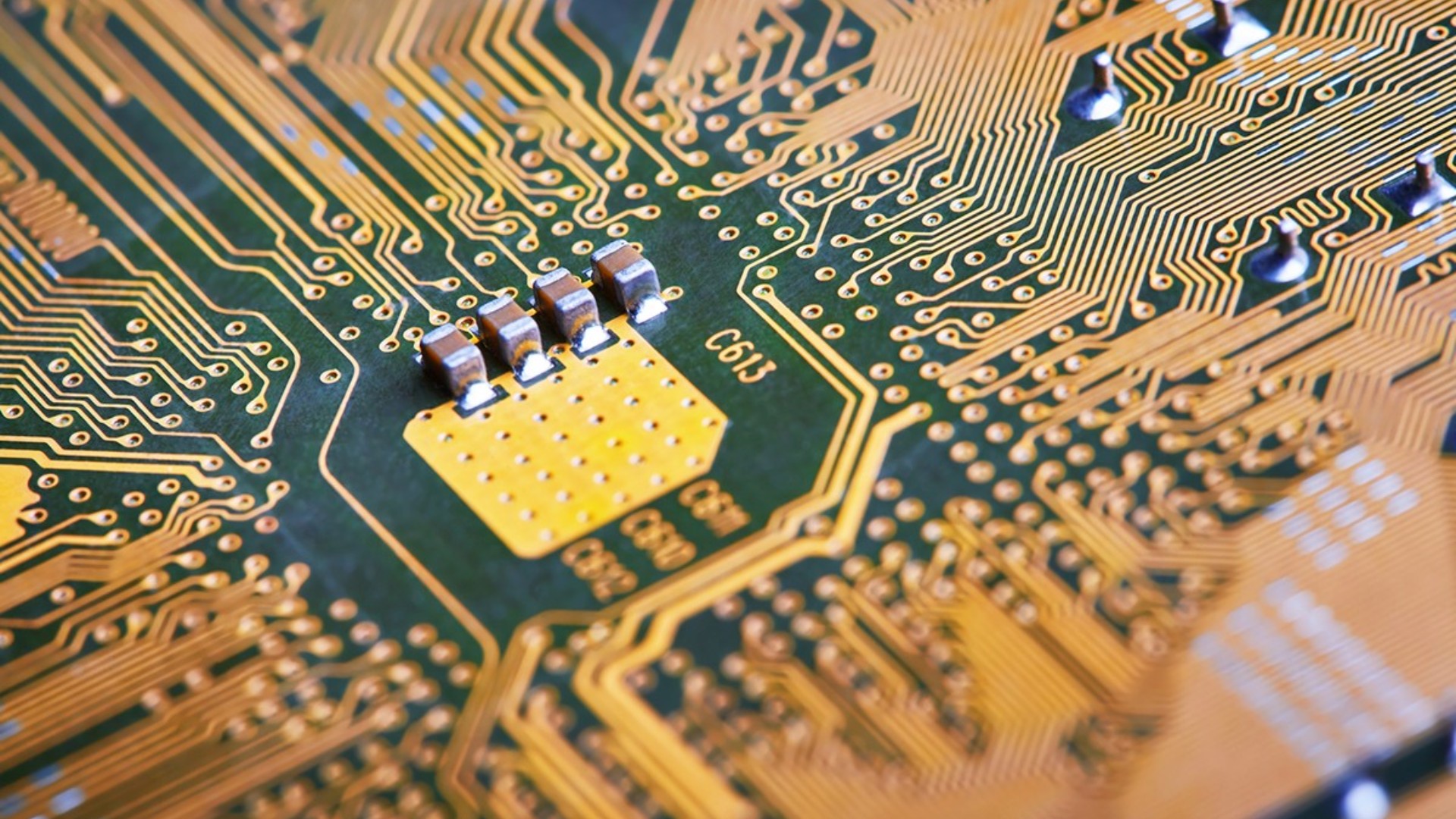
- Conductive Materials: These materials are used to create the conductive traces and pads on the PCB. The most common conductive material is copper, but other materials like aluminum, gold, and silver may also be used in specific applications.
- Solder Masks: These are protective coatings applied over the conductive layers to insulate and protect them from environmental factors and short circuits.
- Silkscreen Legends: These are markings and labels printed on the PCB for identification and assembly purposes.
- Solder Materials: These include lead-based and lead-free solder alloys used for creating interconnections between components and the PCB.
- Conformal Coatings: These are protective coatings applied over the entire PCB assembly to provide additional insulation and environmental protection.
Factors Influencing the Selection of PCB Materials
The choice of PCB materials is governed by several factors, including:
- Electrical Properties: Materials must have suitable electrical properties, such as dielectric constant, loss tangent, and voltage breakdown strength, to ensure proper signal integrity and performance.
- Thermal Properties: PCB materials should have appropriate thermal conductivity and coefficient of thermal expansion (CTE) to dissipate heat effectively and minimize warping or stress on components.
- Mechanical Properties: Materials must possess sufficient strength, rigidity, and dimensional stability to withstand various mechanical stresses during manufacturing, assembly, and operation.
- Environmental Conditions: PCB materials should be resistant to moisture, chemicals, and temperature extremes to ensure long-term reliability in different operating environments.
- Cost: Cost is a significant factor, especially in consumer electronics and high-volume applications, where material selection must strike a balance between performance and affordability.
- Regulatory Compliance: Certain materials may be restricted or banned due to environmental or health concerns, necessitating the use of compliant alternatives.
Popular PCB Materials
1. FR-4
FR-4 is the most widely used substrate material for PCBs in various applications, including consumer electronics, telecommunications, and automotive industries. It is a composite material made of woven fiberglass reinforced with epoxy resin. FR-4 offers excellent electrical insulation, mechanical strength, and dimensional stability, making it a versatile choice for many PCB designs.
2. Polyimide
Polyimide is a high-performance polymer known for its exceptional thermal resistance, chemical resistance, and dimensional stability. It is often used in specialized applications such as aerospace, military, and high-temperature environments where FR-4 may not be suitable. However, polyimide is more expensive than FR-4 and may require specialized manufacturing processes.
3. CEM
Composite Epoxy Materials (CEM) are a class of materials designed to offer improved performance over traditional FR-4. CEMs can have higher glass transition temperatures, better electrical properties, and enhanced thermal conductivity. They are often used in high-frequency applications, such as telecommunications and radar systems, where superior signal integrity is required.
4. Aluminum and Ceramic
Aluminum and ceramic substrates are typically used in specialized applications where high thermal conductivity and dissipation are critical. These materials are commonly found in power electronics, LED lighting, and high-power RF applications. While they offer excellent thermal management, they are generally more expensive and require specialized manufacturing processes.
5. Conductive Materials
Copper is the most commonly used conductive material for PCB traces and pads due to its excellent electrical conductivity, affordability, and ease of processing. However, in specialized applications or harsh environments, alternative materials like aluminum, gold, or silver may be used for their improved corrosion resistance or electrical properties.
Manufacturing Processes for PCB Materials
The manufacturing processes for PCBs involve various steps, including:
- Lamination: In this process, the substrate material (e.g., FR-4) is combined with conductive layers (typically copper foil) using heat and pressure to form a rigid, multi-layered structure.
- Patterning: The conductive layers are selectively etched away using chemical or mechanical processes to create the desired circuit pattern.
- Drilling: Holes are drilled or punched into the PCB to accommodate components and create interconnections between layers.
- Plating: Conductive materials, such as copper, are deposited onto the drilled holes and conductive layers to facilitate electrical connections.
- Surface Finishing: Additional processes, such as solder masking, silkscreen printing, and conformal coating, may be applied to enhance functionality, protection, and aesthetics.
- Assembly: Electronic components are mounted onto the PCB, and interconnections are established using soldering or other assembly techniques.
Environmental and Regulatory Considerations
As the electronics industry continues to evolve, there is an increasing focus on sustainability and environmental responsibility. Regulatory bodies and industry standards have been established to ensure the safe and responsible use of PCB materials. Some key considerations include:
- Restriction of Hazardous Substances (RoHS): This directive aims to restrict the use of certain hazardous materials, such as lead, mercury, and cadmium, in electronic products to minimize environmental impact and protect human health.
- Waste Electrical and Electronic Equipment (WEEE): This directive addresses the proper disposal and recycling of electronic waste, promoting the responsible management of end-of-life electronic products.
- Halogen-Free Materials: There is a growing trend towards the use of halogen-free PCB materials, as certain halogenated compounds (e.g., brominated flame retardants) have been linked to environmental and health concerns.
- Conflict Minerals: Regulations aimed at ensuring the responsible sourcing of certain minerals, such as gold, tantalum, tin, and tungsten, are in place to prevent the financing of armed conflicts and human rights abuses.
Manufacturers and designers must stay informed about these regulations and industry standards to ensure compliance and promote sustainable practices in the production and use of PCB materials.
Emerging Trends and Future Developments
The PCB industry is continuously evolving, driven by technological advancements and changing market demands. Some emerging trends and future developments in PCB materials include:
- High-Frequency Materials: As electronics continue to operate at higher frequencies, there is a growing need for materials with superior electrical properties, such as low dielectric loss and controlled impedance, to maintain signal integrity.
- Flexible and Stretchable Materials: The rise of wearable electronics and Internet of Things (IoT) devices has fueled the development of flexible and stretchable PCB materials that can conform to various shapes and withstand mechanical stresses.
- Thermal Management Materials: As electronic devices become more compact and powerful, effective thermal management is crucial. Research is underway to develop PCB materials with enhanced thermal conductivity and heat dissipation capabilities.
- 3D Printing and Additive Manufacturing: The integration of 3D printing and additive manufacturing techniques in PCB production opens up new possibilities for complex geometries, rapid prototyping, and customized designs.
- Bio-based and Sustainable Materials: There is an increasing focus on developing eco-friendly and sustainable PCB materials derived from renewable resources, such as bio-based resins and natural fibers, to reduce the environmental impact of electronics manufacturing.
As technology continues to advance, the demand for innovative and high-performance PCB materials will continue to drive research and development efforts in this field.
Frequently Asked Questions (FAQs)
- What is the difference between FR-4 and CEM? FR-4 is a traditional and widely used substrate material made of woven fiberglass reinforced with epoxy resin. CEM (Composite Epoxy Material) is a more advanced material designed to offer improved performance over FR-4, such as higher glass transition temperatures, better electrical properties, and enhanced thermal conductivity. CEMs are often used in high-frequency applications where superior signal integrity is required.
- Why is polyimide used in specialized applications? Polyimide is a high-performance polymer known for its exceptional thermal resistance, chemical resistance, and dimensional stability. It is often used in specialized applications such as aerospace, military, and high-temperature environments where traditional materials like FR-4 may not be suitable. However, polyimide is more expensive and may require specialized manufacturing processes.
- What are the advantages of using aluminum or ceramic substrates? Aluminum and ceramic substrates offer excellent thermal conductivity and dissipation capabilities, making them suitable for applications where effective heat management is critical, such as power electronics, LED lighting, and high-power RF applications. However, these materials are generally more expensive and may require specialized manufacturing processes.
- What is the role of solder masks in PCB construction? Solder masks are protective coatings applied over the conductive layers on a PCB. They serve two primary functions: insulating the conductive traces from each other to prevent short circuits, and protecting the conductive layers from environmental factors such as moisture, chemicals, and abrasion.
- What are the environmental and regulatory considerations regarding PCB materials? There are several environmental and regulatory considerations related to PCB materials, including the Restriction of Hazardous Substances (RoHS) directive, which restricts the use of certain hazardous materials like lead and mercury; the Waste Electrical and Electronic Equipment (WEEE) directive, which addresses proper disposal and recycling of electronic waste; and regulations aimed at ensuring responsible sourcing of conflict minerals. Additionally, there is a growing trend towards the use of halogen-free and bio-based materials to promote sustainability and reduce environmental impact.
By addressing these frequently asked questions, we have provided insights into the key aspects of PCB materials, their properties, applications, and the factors influencing their selection.


