USB Type-C has rapidly become the universal standard for wired data transfer and power delivery. Its reversibility, compact form factor and versatility make USB-C ideal for connecting peripherals to desktops, laptops, smartphones and other electronics. Integrating a USB-C connector in a printed circuit board (PCB) enables transferring high speed data, delivering power up to 100W and facilitates a unified user experience.
This article provides a step-by-step guide on integrating a USB-C connector in a PCB design. We will cover USB-C signals, connector selection, PCB layout considerations, schematic design, cable assembly and test steps to help you expertly add USB-C capability to your next product’s PCB.
Overview of USB-C Connector

The USB Type-C connector replaces larger USB-A and USB-B versions with a compact, reversible design. Its key characteristics include:
- Compact form factor – 8.4mm height x 2.6mm width
- Reversible plug orientation
- Friction fit – No clasps or springs
- Durability – 10,000 insertions
- High speed data transfer up to 10Gbps
- Power delivery up to 100W
- Alternate modes like DisplayPort, HDMI, Thunderbolt support
USB-C connector features a compact, reversible design (Image Credit: TE Connectivity)
USB-C achieves this flexibility using 24 pins to support diverse applications. Intelligent design allows unused pins to be powered off for simpler applications.
USB-C Signals and Pins
The USB-C connector has 24 pins, numbered B1 through B12 on one side and A1 through A12 on the flip side:
USB Type-C connector pinout showing both sides (Image Credit: USB-IF)
Here are the key signals allocated to these 24 pins:
Power Delivery (PD)
- VBUS – Power transfer up to 5A at 20V (100W)
- GND – Ground return for power and signals
USB 2.0 Data
- D+ and D- differential signals for USB 2.0 data
USB 3.2 Gen 1/Gen 2 Data
- TX1+/TX1- and TX2+/TX2- differential pairs for USB data
Configuration Channel (CC)
- CC1 and CC2 for connection management and power negotiation
Other Signals
- SBU – USB OTG (On-The-Go) role switching
- VCONN – Power for active cable electronics
The flexible pin usage allows supporting just the needed functions for a given product, while maintaining future compatibility.
USB-C Connector Selection
A range of USB-C connector options are available from vendors like TE Connectivity, Molex, JAE Electronics, Amphenol and Wurth Elektronik. Factors to consider when selecting a USB-C connector include:
Mounting Style
- Through-hole – For attaching directly to PCB
- Surface mount – Allows mounting on surface of PCB
- Mid-mount – Combination through-hole and surface mount
Shielding
- No shield – Lowest cost but provides no EMI protection
- Partial shield – Only over connector tongue for partial EMI protection
- Full shield – Shields entire connector for greatest EMI protection
Temperature Rating
- Standard: -20°C to +85°C
- Industrial: -40°C to +105°C
- Extended: -55°C to +125°C
Current Rating
- 3A, 5A or 10A current rating for power delivery
Accessories
- Flanges, cable clamps, panel mounts, waterproof seals etc.
For most applications, a through-hole or mid-mount connector with partial shielding works well. Select ratings and accessories tailored for your product requirements.
PCB Layout Design
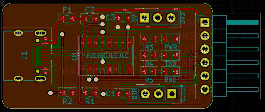
Careful PCB layout is crucial for achieving reliable performance when integrating any high speed connector like USB-C:
Place Near Edge of PCB
Place the USB-C connector as close to the edge of the PCB as possible. This minimizes the trace length from connector to the routing layers.
Minimize Trace Length Differences
Keep the differential pair trace lengths matched to within 25 mils between USB 2.0, USB 3.2 and CC signals. Mismatched lengths can cause data errors.
Use Controlled Impedance Traces
Set trace impedances to 90Ω ± 10% for the high speed differential traces using impedance calculators. This prevents signal reflections.
Include Ground Vias Under Connector
Connect all connector ground pins to the ground plane using multiple vias placed close together. This improves return current flow.
Include Stabilizing Components
Add capacitors, ferrite beads, damping resistors and other components to prevent resonances and oscillations. Follow manufacturer guidelines.
Use Minimum Spacing
Route signals at minimum spacing between traces and to adjacent layers. This allows return current to flow closely.
Limit Plane Cuts Under Connector
Avoid cuts in the ground plane under the connector to maintain continuous shielding. Use stitching vias if cuts are unavoidable.
Follow Keepout Rules
Respect the connector keepout area under and around the part in placement and routing. Prevent traces crossing underneath.
By following sound high speed layout techniques, the USB-C interface can achieve flawless performance up to 10Gbps speeds.
Schematic Design Tips

The schematic connects the USB-C connector symbol to surrounding components correctly to support the desired functions:
Select Right Connector Symbol
Use the USB-C connector symbol from your schematic library showing all 24 pins. Connect the pins to match the layout.
Show Power Input
Connect the VBUS pin to the incoming power rail from the voltage regulator stage.
Connect Grounds
Join the connector shield and all ground pins to the board’s ground network with multiple connections.
Route Configuration Channel
Route the CC1 and CC2 pins to pull-up/pull-down resistors and then to device CC logic.
Include TVS Diodes
Use transient voltage suppressor (TVS) diodes between VBUS and ground for overvoltage protection.
Add ESD Protection
Use ESD protection diodes on the high speed differential lines to prevent static damage.
Consider Data Direction
If defining as host vs device, set up D+ and D- appropriately for the design scenario.
Add Test Points
Test points on VBUS, D+/D- and CC pins enable validating signals.
Taking care with the schematic ensures the USB-C connectivity provides robust performance in the final application.
USB-C Cable Assembly
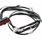
A USB-C cable connects the PCB to peripherals or a host system. Here are some best practices for USB-C cable assembly:
Choose Quality Shielded Cable
Use a cable with braided shielding to contain EMI. Ferrite cores help suppress common mode noise.
Check Cable Wiring
Verify cable wires connect correspondingly between plugs following USB-C pinout standards.
Validate Compatibility
Test plugs with actual mating receptacles to confirm proper fit, keying and retention strength.
Include E-Marker Chip
An e-marker chip in the plug carries identifying information for the cable. Programs PD capability.
Minimize Bend Radius
Maintain >4x cable diameter bend radius to avoid damaging wire strands and insulation.
Consider Strain Relief
Well designed strain relief prevents cable tension damage during handling.
Validate Gauge and Length
Meet specified limits on cable wire gauge and end-to-end length to avoid power loss or data errors.
Care with cable assembly prevents connectivity issues or degraded performance.
USB-C Integration Testing

Once the PCB design and cable are complete, systematic testing verifies proper USB-C performance:
Continuity Testing
- Confirm connectivity through every contact using a multimeter probe or continuity tester.
Power Delivery Validation
- Verify negotiated PD voltage and current levels meet expected values.
Data Throughput Testing
- Perform data transfers at increasing speeds and measure throughput, errors, latency.
Signal Integrity Testing
- Use an oscilloscope or protocol analyzer to view and tune USB-C signals.
Interoperability Testing
- Test against vendor-specific cables and devices to catch interoperability issues.
Stress Testing
- Run repeated insertions and long duration plugged-in tests to validate robustness.
Error Condition Testing
- Simulate overcurrent, ESD, EMI events to confirm proper fault response.
Rigorous testing is vital for delivering a robust, reliable USB-C implementation that seamlessly interconnects with peripherals and host systems.
Conclusion
USB-C integration unlocks ubiquitous connectivity, speedy data transfers and flexible power delivery for next generation electronics. Careful schematic, layout, component selection and validation lays the foundation for a successful USB-C PCB implementation. Leveraging the guidance in this article will help you harness the full potential of USB-C in your designs and delight your end users with an intuitive, dependable experience.
Frequently Asked Questions
Q1: Does USB-C require any specific PCB stackup?
A1: USB-C does not require specific PCB layer counts or stackup. Good ground plane distribution and proper impedance control for signal traces are most important. 4-6 layer designs work well.
Q2: How do I determine the right current rating for USB-C power?
A2: Budget 3-5A for phones/tablets, up to 10A for laptops and higher for power tools, appliances etc. Size cables and PCB traces accordingly.
Q3: Can a USB 2.0-only device use USB-C connectors?
A3: Yes, USB-C can support USB 2.0 using only the D+ and D- signals. This provides reversibility without high speed.
Q4: Does USB-C need shielding on the PCB?
A4: Partial shielding over the connector tongue helps reduce EMI. Additional board-level shielding depends on EMI requirements.
Q5: Can I probe live USB-C signals with an oscilloscope?
A5: It is not recommended to probe USB-C differential signals directly due to risk of damage. Use a protocol analyzer with high impedance taps.

