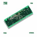
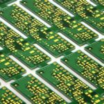
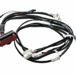
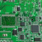
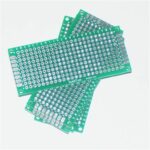
Flexible printed circuit (FPC) is a type of printed circuit board that is made of a thin, flexible material such as polyimide or polyester. FPCs allow for connections between electronics in applications where rigid boards would not be suitable. They are commonly used in consumer electronics, medical devices, automotive electronics and more.
FPCs can have multiple conductive layers, typically ranging from 1 to 12 layers. The number of layers in an FPC depends on the complexity and interconnect requirements of the application. 4-layer FPCs provide more interconnect capabilities compared to 2-layer FPCs, while still maintaining good flexibility and bend radius properties.
4-Layer FPC Construction

A 4-layer FPC consists of a flexible dielectric base material that is laminated with conductive copper layers on both sides. Here is a breakdown of the different layers in a 4-layer FPC:
Layer 1 – Coverlayer
The topmost layer of a 4-layer FPC is called the coverlayer or covercoat. This layer provides insulation and protection for the conductive copper traces. The coverlayer material is typically a thin polyimide film. It can be coated with an acrylic or epoxy-based adhesive on one side to bond to the other layers. The coverlayer has openings or windows in areas where components need to be soldered or contacts need to be exposed.
Layer 2 – Upper traces
Under the coverlayer is the upper copper layer that contains the conductive traces and interconnects. This layer is patterned using lithographic processes to produce the circuit patterns. The traces are etched from a thin rolled annealed copper foil, typically around 18-35 μm thick. A surface finish like immersion silver, immersion tin or organic solderability preservative (OSP) is applied to protect the copper from oxidation and improve solderability.
Layer 3 – Inner traces
The third layer contains the inner copper traces sandwiched between the dielectric base layers. For a 4-layer FPC, there are two inner layers. Vias or plated through holes connect traces between the different layers. The inner trace layers are fabricated similar to the outer layers with lithographic patterning and etching.
Layer 4 – Dielectric core
At the center of the stackup is the flexible dielectric base material that provides mechanical support. Polyimide is the most common type of dielectric used, but other options include polyester (PET), polyethylene naphthalene (PEN), polyphenylene sulfide (PPS) and others. The dielectric thickness typically ranges from 13μm to 75μm. Adhesives bond the dielectric core to the copper foil layers.
Layer 5 – Lower traces
Under the dielectric core is the second inner trace layer. It is fabricated identical to the upper inner layer. The two inner layers are circuit patterns etched from copper foil.
Layer 6 – Adhesive
The bottom adhesive layer bonds the lower copper foil layer to the dielectric base material. Epoxy or acrylic adhesives are commonly used. The adhesive must be flexible to allow FPC bending.
Layer 7 – Lower traces
The bottom layer contains the lower traces and interconnects. It is fabricated using the same lithographic patterning and etching process as the upper foil layer.
Layer 8 – Adhesive
This adhesive layer bonds the bottom traces to the bottom cover layer. It provides insulation between the lower circuitry and coverlayer.
Layer 9 – Coverlayer
The bottom coverlayer or covercoat provides insulation and protection for the bottom traces. It is a thin polyimide film like the top coverlayer. Openings in the coverlayer allow for component solding and contact areas.
So in summary, a 4-layer FPC contains 2 signal layers on each side of a dielectric base material. Signal layers are etched copper circuitry patterns. Vias interconnect the inner and outer trace layers. Coverlayers insulate and protect the traces. Adhesives bond between the layers.
Benefits of 4-Layer FPCs
Four-layer FPCs offer several benefits compared to 2-layer FPCs:
- Higher circuit density: With two extra inner layers, 4-layer FPCs can accommodate more complex circuit routing in the same footprint. More components and finer traces can be packed into a compact flexible board.
- Impedance control: The multiple reference planes provided by the ground layers better controls electrical impedance. This allows for higher frequency signals.
- Low EMI: Additional grounded layers shield signals and contain electromagnetic interference (EMI). This is important for sensitive circuits.
- Higher current capacity: The copper layers are divided into signal and ground planes. This allows higher current flow as grounds have larger traces.
- Thinner dielectric: With two dielectric cores, thinner overall material can be used compared to 2-layer FPC while maintaining isolation and insulation.
- Stiffness control: Dielectric materials and thicknesses can be selected to tune the flexural stiffness. 4-layer FPCs can be made stiffer than 2-layers.
- Component embedding: The extra layers provide space to embed passives or actives within the PCB through cavities or cutouts.
Overall, the four conductive layers give more flexibility (no pun intended!) in FPC design and layout. This allows for more complex circuits to be integrated while still retaining the benefits of a thin, lightweight and flexible board.
4-Layer FPC Applications
Some common applications that utilize 4-layer FPC technology include:
Consumer Electronics
- Flex circuits for laptop and notebook PCB interconnects
- Display driver electronics in mobile phones and tablets
- Foldable or rollable OLED display interconnections
- Flexible printed antennas ( antennas do not have to be rigid anymore)
- Wearable device flex PCBs
- Flex-to-board connectors
Automotive Electronics
- Flexible circuitry for cameras, sensors, infotainment and control units
- Seat heaters with flex circuits integrated into upholstery
- Overhead console flex circuits
- Ignition switch interconnects
- Harness assemblies with high density flex jumpers
Medical Devices
- Hearing aids and cochlear implants
- Wearable health monitors (ECG, respiration, etc)
- Endoscopes and catheter flex PCBs
- Surgical tools with embedded flex boards
- Implants such as pacemakers and neurostimulators
Industrial
- Flexible interconnects on moving parts for robotics
- NDT array probes
- Avionics and aerospace sensors
- Non-rigid antennas
So in summary, 4-layer FPCs are well suited for compact electronics in dynamic bending applications across many industries. The four conductive layers enable complex circuitry and routing while maintaining excellent flexibility.
4-Layer FPC Design Considerations

Here are some important design factors to consider when working with 4-layer flex circuits:
Dielectric Material
The dielectric material type and thickness influences flexibility. Thinner polyimide allows for tighter bending radii down to 0.10mm, while thicker polyimide or polyester gives more stiffness. Materials with higher glass transition temperatures withstand repeated dynamic flexing.
Trace Width/Spacing
Narrower traces with finer spacing permits higher densities, at the expense of higher cost. Typical trace/space is 100μm (4 mils) and above. Finer geometries are possible for specialized applications.
Bend Radii
Sharp corners should be avoided. Bend radii should be 2-3X the FPC stackup thickness. Vias at bend locations require additional radius.
Layer Stackup
The layer count, dielectric materials and thicknesses determine stiffness. Thicker overall stackups limit bendability. Stackups should be optimized for flexibility requirements.
Landing Pads
Sufficient landing pads must surround vias and component pads to account for layer misalignment during lamination. This is especially important for components in bend areas.
Adhesives
Adhesive type and thickness affects flex performance. Adhesives should withstand dynamic and thermal cycling without cracking or delaminating.
Test Points
Include text points connected to traces for validation and debugging. Exposed copper at test points needs to be compatible with probing.
Panel Utilization
Smaller circuits can be arrayed on panel sizes up to 510mm x 510mm for cost-effective volume production. Larger or complex boards may need individual panels.
Solder Mask
Solder mask openings should account for layer misalignment and provide sufficient trace coverage for protection while allowing soldering.
Proper design considering these factors will ensure reliable, functional 4-layer flex circuits that maximize the benefits of flexible PCBs.
4-Layer FPC Fabrication Process
4-layer FPCs follow a lithographic fabrication process similar to rigid PCBs but using flexible materials able to withstand dynamic bending. Here is a general overview of the 4-layer flex manufacturing process:
- Copper Foil Lamination – Rolls of copper foil are bonded to dielectric polyimide materials using adhesive. FPCs typically use rolled annealed copper foil.
- Drilling – For boards with through hole vias, a laser drills thousands of microscopic holes through the layers.
- Via Metallization – The via holes are plated with an electroless copper process to metallize the interior barrel surfaces.
- Photolithography – Each layer is coated with a photosensitive resist coating. An imaging process exposes the resist.
- Developing – The resist is developed, which removes the unexposed areas to create the circuit pattern.
- Etching – Ferric chloride solution etches away the unwanted copper, leaving only the traced copper circuitry.
- Resist Stripping – The remaining photoresist is stripped away.
- Outer Layer Imaging – Additional layers are processed to image the outer layer circuitry.
- Stackup Lamination – The flexible copper layers are precisely aligned and laminated together using heat and pressure.
- Singulation – The large panel goes through a punching process to release individual circuits.
- Testing – Each board is electrically tested. Automated optical inspection checks for defects.
- Finishing – Carbon ink or other coatings are applied to provide insulation and marking.
This multi-step process leverages typical PCB fabrication techniques to produce multilayer flex circuits. Each step must be carefully controlled to manufacture high quality, reliable 4-layer FPCs.
Summary
Four-layer flexible PCBs provide an optimal balance of flexibility, density and performance. The four conductive layers enable complex routing while maintaining excellent dynamic bendability. Polyimide is commonly used as the flexible dielectric material. A 4-layer stackup contains two signal layers on each side of central dielectric cores with adhesive between the layers. The lithographic fabrication process allows high density traces and small features. 4-layer FPCs are widely used for interconnects in consumer electronics, automotive, medical, industrial and aerospace applications. With good design practices, 4-layer flex circuits can maximize integration while providing dynamic flex capability and reliability.
Frequently Asked Questions
What is the typical thickness of a 4-layer FPC?
The overall thickness of a 4-layer FPC generally ranges from about 75 to 125 microns (3 to 5 mils). However, thickness can vary depending on the materials used. Polyimide dielectric layers are typically around 25-50 microns each. Adding 2 layers of rolled copper at 18-35 microns per side results in the total stackup thickness.
What are the different types of flexible circuit materials?
The most common dielectric materials used are polyimide, polyester (PET), polyethylene naphthalate (PEN), and polyphenylene sulfide (PPS). Polyimide provides the best thermal properties and flexibility. Other exotic materials like PEEK or Kapton are also sometimes used.
What are some key considerations when laying out 4-layer FPC?
Important layout factors are: minimizing 90 degree bends, using large bend radii, providing sufficient landing pads, allowing for layer misalignment tolerance, accounting for proper adhesive openings, and providing test/probe points.
What are the typical resolutions for traces/spaces in 4-layer FPC?
Typical trace widths and spaces for 4-layer FPCs range from 100 microns (4 mils) and above. Specialized processes can pattern finer geometries down to around 50 microns (2 mils) trace/space.
How many flex layers would be needed for a complex application?
For very complex, high density routing, FPCs up to 12 layers can be produced. But this reduces flexibility. 4-6 layers will accommodate most interconnect requirements while maintaining good bendability. High complexity may require rigid-flex boards.
What are the key differences between rigid and flex PCBs?
Rigid PCBs use FR-4 and other rigid laminates while flex PCBs use polyimide and flexible plastics. Flex PCBs are thinner, dynamically bendable and require special handling and processes. Rigid PCBs offer better thermal performance and component mounting.
How are components assembled onto 4-layer FPCs?
Common assembly methods include soldering, conductive adhesives, thermocompression bonding, and mechanical attachments. Reflow soldering is most typical for SMT parts. Selective wave soldering can solder through-hole components. Fully automated assembly lines are usually required.
What are important FPC testing considerations?
Testing requires specialized fixturing to avoid bending damage with probes. Low contact forces are necessary. Continuity testing checks layer-to-layer interconnections and vias. Automated optical inspection of solder joints and assembly is recommended.
What are typical FPC and flex circuit applications?
FPCs are widely used in consumer electronics, computing, telecom, automotive, medical, military/aerospace and industrial applications. Usage ranges from dynamic flex interconnects to static rigid-flex boards. Any application requiring thin, light and flexible PCBs can benefit from FPCs.

