Thermoelectric modules (TEMs) use the Peltier effect to provide precise heating or cooling capabilities without liquids or gases. The active thermoelectric elements are mounted between two substrates that transfer heat – typically a metal base and a printed circuit board. The substrate combination is key for managing the thermal load. Copper is an ideal base material paired with a thermoelectric PCB to optimize performance in thermoelectric assemblies.
This article looks at what thermoelectric copper base PCBs are, how they work, design considerations, manufacturing processes, assembly, applications, pros/cons compared to alternatives like Aluminum or Ceramics, and frequently asked questions.
What is a Thermoelectric Module?
A thermoelectric module consists of N-type and P-type semiconductor pellets wired electrically in series and sandwiched between two ceramic substrates. Applying DC power drives heat absorption on the cold side and heat dissipation on the hot side proportional to current based on the Peltier effect.
Role of the Metal Base in a TEM
The top substrate of a TEM is typically a PCB while the bottom substrate is metal like Copper or Aluminum. The metal base serves several key functions:
- Provides excellent thermal conduction to remove heat from hot pellets
- Allows straightforward mounting to heat sinks or surfaces
- Adds structural rigidity to support TEM pellets
- Can include mounting holes for easy installation
- Gives flat smooth surface for pellet bonding
Copper offers the best performance as a thermoelectric base material due to its superior thermal properties.
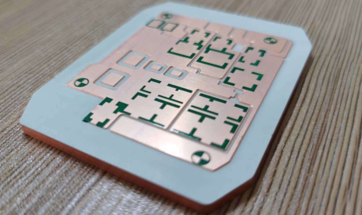
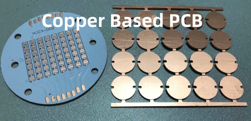
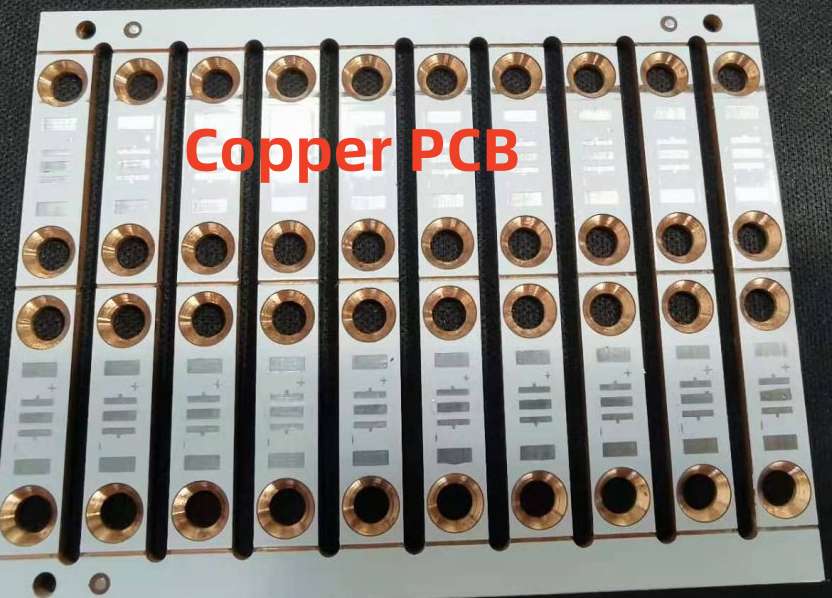
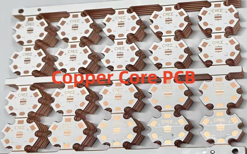
What is a Thermoelectric Copper Base PCB?
A thermoelectric copper base PCB consists of a thermoelectric module mounted onto a printed circuit board substrate with a copper base plate on the opposite side:
The PCB provides electrical connectivity and structural support while the copper base removes heat. The combination allows creating customizable thermoelectric assemblies.
Pros and Cons of Using Copper Base PCBs
Copper base PCBs offer the following advantages versus alternatives like Aluminum or Ceramics:
Pros
- Excellent thermal conductivity for heat dissipation
- Allows custom PCB for electrical routing and interconnect
- Eases integration and device packaging with standard PCB processes
- Readily available at lower cost than exotic materials
- Easy to solder components and attach terminals
- Can incorporate thermal vias and planes in PCB
Cons
- Heavier than Aluminum or Ceramic bases
- Less stiff than ceramic and prone to vibration issues
- Care required during assembly to avoid damage to copper base
- Higher CTE mismatch versus ceramic requiring analysis
- Not suitable for very high temperature applications
Thermal Design Considerations
Key considerations when designing thermoelectric copper base PCB assemblies:
- Carefully model the thermal load and select suitable TEMs to handle it
- Optimize copper thickness and PCB dielectric layers as heat spreaders
- Incorporate thermal vias under hot spots
- Select a thermally conductive dielectric material (FR-4, Polyimide, etc)
- Manage thermal interface material (TIM) between base and heat sink
- Consider heat dissipation needs – heatsink, coldplate, fan, etc
- Evaluate alignment of PCB traces to minimize hot crossover
- Analyze thermomechanical stresses due to CTE mismatches
- Predict maximum temperatures during operation and test limits
Thorough thermal design is imperative to leverage the heat transfer capability of the copper base.
Manufacturing Process for Copper Base PCBs
Fabricating a thermoelectric copper base PCB involves:
- Standard PCB fabrication with desired dielectric layers
- CNC machining a copper plate to required dimensions
- Precisely thinning the plate to optimal thickness
- Cleaning and surface preparation of the plates
- Applying bonding film between PCB and copper base
- Using thermal compression bonding to laminate the copper plate to the PCB
- Tuning the pressure and temperature to achieve high bond strength
- Inspecting the laminated assembly for voids or gaps at interface
- Testing bond shear strength and thermal impedance
The integrity of the PCB-to-base bond critically impacts performance. Careful process controls are needed to avoid internal stresses or delamination over thermal cycles.
Thermoelectric Assembly Process Steps
Typical assembly process flow when constructing a thermoelectric copper base PCB module:
- Solder thermistors onto PCB for temperature monitoring
- Dispense thermally conductive adhesive onto copper base
- Precision place thermoelectric pellets onto adhesive areas
- Make electrical interconnects between TEM and PCB
- Attach heat sink to copper base side with thermal interface material
- Apply epoxy or hardware to secure components mechanically
- Plug housings and wire terminations for electrical connections
- Perform thermal validation testing across operating temperatures
- Program and calibrate thermistor monitoring and control
The assembly is usually automated but can be manual. Verification testing ensures the device performs to thermal specifications.
Example Applications of Thermoelectric Copper Base PCBs
Some common applications leveraging thermoelectric copper base PCB assemblies include:
- Precise temperature control of diode lasers
- Maintaining setpoint temperatures in medical diagnostic devices
- Cooling electronic components like CPUs or power devices
- Stabilizing oven temperatures in lab instruments
- Portable cooling boxes for transporting temperature-sensitive pharmaceuticals
- Lowering battery temperatures in electric vehicles during charging
- Catering food trolleys heating/cooling prepared food
Any application requiring accurate, responsive temperature control without needing potential leaks from liquid cooling can benefit from thermoelectrics.
Comparison to Aluminum and Ceramic Bases
Versus alternative base materials:
- Aluminum offers lighter weight and lower cost but has around 30% lower thermal conductivity than copper reducing heat transfer. It also has a higher CTE mismatch.
- Ceramic provides greater dimensional stability across temperature due to lower CTE but has 70% lower thermal conductivity than copper further limiting heat dissipation. It is also heavier than aluminum and far more expensive.
- Copper offers the best thermal performance and reasonable cost but density is higher than aluminum. It must be carefully joined to minimize CTE-induced stresses.
Thermoelectric PCB Design Recommendations
Recommendations when designing the PCB portion of a thermoelectric assembly:
- Use minimum 2-layer PCB for power and ground plane stability but 4-6 layers optimal
- Assign one layer as continuous ground plane for low loop inductance
- Ensure power plane coverage suits current levels
- Incorporate thermal vias under hot components to conduct heat to base
- Select thermally conductive PCB substrate material
- Define keepout zones for thermoelectric elements
- Include temperature monitoring thermistors in key locations
- Add several fiducials for pick and place alignment
- Allow clearance for mechanical attachment of housing
- Review layout for thermal and mechanical stresses
Thermoelectric Long Term Reliability Factors
Some key factors impacting long term thermoelectric assembly reliability:
- Thermal cycling induced stresses from CTE mismatches causing substrate or joint cracks
- Shock and vibration loads creating mechanical stress on joints
- Material compatibility across temperature range and thermal gradients
- Solder joint integrity and metallurgical interdiffusion effects
- TEM solder voiding leading to hotspots and failures
- Degradation or breakdown of thermal interface materials
- Environmental seals preventing moisture ingress
- Electrical contact resistance stability over thousands of hours
- Adhesion strength reduction through long term exposure
Extensive reliability testing across operating conditions ensures a robust product lifetime.
Summary
- Thermoelectric copper base PCBs utilize copper’s excellent thermal properties to dissipate heat.
- A PCB provides interconnect and customization while the copper base removes heat.
- Thermal modeling guides design while advanced PCB processes enable fabrication.
- Assembly requires precision TEM placement and thermally conductive joints.
- Copper base TEMs serve applications needing precise temperature control.
- Copper offers better performance than cheaper Aluminum or more costly Ceramic bases.
When designed properly, thermoelectric copper base PCBs provide unmatched thermal regulation in a small, customizable package.
Frequently Asked Questions
What PCB substrate materials work best for thermoelectric modules?
Higher thermal conductivity dielectrics like polyimide, FR-4, Isola, and metal-core boards are preferred. Ceramics can also be direct-bonded for maximum performance but at higher cost.
What are recommended PCB layer counts for thermoelectrics?
A minimum 2-layer PCB is required, with 4 to 6 layers typical for optimal power distribution and thermal performance. This provides ground and power planes while avoiding excessive dielectric insulation.
What construction is best to thermally link PCB layers with the base?
Abundant thermal vias under hot components that connect all layers is recommended. Alternating these vias to form “thermal pillars” through all layers provides the most effective vertical heat conduction path to the base plate.
How are thermoelectric modules electrically interconnected with the PCB?
TEM pellets are usually soldered to PCB pads allowing reliable electrical connectivity. Alternatives like conductive epoxy or spring pins are also possible but introduce higher impedance or use restrictions.
What problems occur when thermoelectrics are cycled to subzero temperatures?
Large deltas and rapid thermal cycling from room temperature down to subzerocan induce substrate cracks from material mismatches. Slow temperature ramp rates and shock absorbing mountings help mitigate these stresses.


