
Introduction
In the ever-evolving world of electronics, the design process plays a crucial role in bringing innovative ideas to life. From conceptualization to manufacturing, the journey of transforming a concept into a tangible product involves several stages, each as important as the next. Two key components of this process are schematic design and printed circuit board (PCB) layout software. These specialized tools have revolutionized the way engineers and designers approach circuit design, streamlining the workflow and enabling the creation of complex and intricate electronic systems.
This comprehensive article delves into the realm of schematic design and PCB layout software, exploring their functionalities, features, and importance in the electronics industry. We will cover various aspects, including the fundamentals of schematic design, the intricacies of PCB layout, and the integration of these two essential components. Additionally, we will discuss the key considerations when selecting the appropriate software tools, industry best practices, and the future trends shaping this dynamic field.
Schematic Design: The Blueprint of Electronic Circuits

Schematic design is the foundation upon which electronic circuits are built. It is a visual representation of the components and their interconnections, serving as a blueprint for the entire circuit. This intricate diagram communicates the functional aspects of the circuit, enabling designers and engineers to analyze, simulate, and troubleshoot before proceeding to the physical implementation stage.
The Importance of Schematic Design
- Clear Communication: Schematics provide a standardized language for conveying circuit designs, ensuring clear communication among team members, manufacturers, and stakeholders.
- Design Validation: By simulating and analyzing the schematic, designers can identify potential issues, optimize performance, and validate the design before committing to physical prototyping or production.
- Documentation and Maintenance: Well-documented schematics serve as valuable references for future modifications, troubleshooting, and maintenance activities.
Key Features of Schematic Design Software
- Component Libraries: Comprehensive libraries containing a vast array of electronic components, from resistors and capacitors to complex integrated circuits, allowing designers to quickly assemble circuits.
- Hierarchical Design: The ability to create hierarchical designs by grouping related components into reusable blocks, enabling better organization and scalability.
- Simulation and Analysis: Integrated simulation tools that allow designers to analyze circuit behavior, perform parametric sweeps, and identify potential issues before physical implementation.
- Design Rule Checking (DRC): Automated checks to ensure compliance with design rules, standards, and best practices, reducing the risk of errors and improving overall quality.
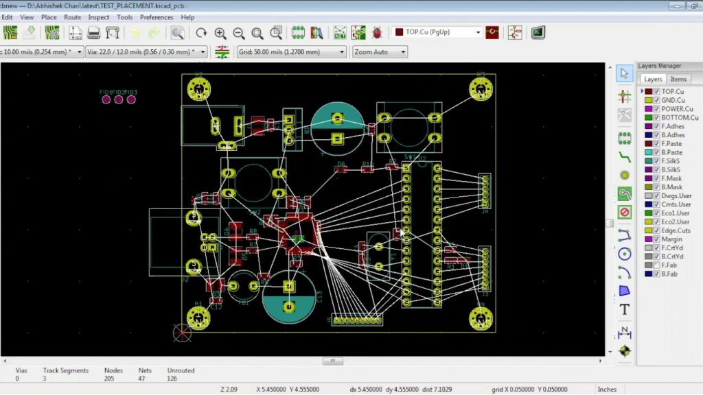
PCB Layout: Translating Schematics into Physical Reality
Once the schematic design is complete, the next step is to translate it into a physical printed circuit board (PCB) layout. This process involves arranging the components and routing the interconnections on a planar surface, taking into account various constraints and design rules. PCB layout software plays a critical role in this stage, enabling designers to efficiently create intricate board designs while adhering to industry standards and manufacturing specifications.
The Importance of PCB Layout
- Signal Integrity: Proper layout techniques ensure signal integrity, minimizing interference, crosstalk, and other signal degradation issues.
- Thermal Management: Effective thermal management through strategic component placement and proper trace sizing, ensuring reliable operation and longevity of the electronic device.
- Manufacturing Compliance: Adherence to manufacturing guidelines and design rules, ensuring compatibility with fabrication processes and minimizing production issues.
Key Features of PCB Layout Software
- Component Placement: Automated and manual placement tools for arranging components on the board while considering factors such as thermal dissipation, signal integrity, and design rules.
- Trace Routing: Advanced routing algorithms and interactive routing tools for creating efficient and error-free interconnections between components.
- Design Rule Checking (DRC): Comprehensive rule checking to ensure compliance with manufacturing specifications, such as clearance requirements, trace widths, and via sizes.
- Signal Integrity Analysis: Integrated tools for analyzing signal integrity, including impedance control, crosstalk simulation, and high-speed design considerations.
- 3D Visualization: Realistic 3D rendering capabilities, allowing designers to visualize the final product and identify potential mechanical issues before manufacturing.
Integration of Schematic Design and PCB Layout
While schematic design and PCB layout are distinct stages in the design process, they are inherently interconnected. Modern software tools facilitate seamless integration between these two phases, enabling a streamlined workflow and efficient data exchange.
Benefits of Integration
- Design Synchronization: Changes made in the schematic are automatically reflected in the PCB layout, and vice versa, ensuring consistency and reducing the risk of errors.
- Cross-Probing: The ability to cross-probe between the schematic and PCB layout, allowing designers to easily navigate and identify corresponding components and connections.
- Design Reuse: Reusable schematic blocks can be imported directly into the PCB layout, saving time and promoting design consistency across projects.
Collaborative Design Environment
Many modern software tools offer collaborative design environments, enabling teams of engineers and designers to work concurrently on the same project. This collaborative approach fosters seamless communication, real-time updates, and efficient design reviews, ultimately leading to faster time-to-market and improved product quality.
Choosing the Right Software Tools
With numerous schematic design and PCB layout software solutions available, selecting the appropriate tool can be a daunting task. Here are some key factors to consider when evaluating software options:
- Design Complexity: Assess the complexity of your projects, considering factors such as board size, component density, and signal integrity requirements, and choose software that can handle your specific needs.
- Integration and Data Exchange: Evaluate the software’s ability to integrate with other tools in your design workflow, ensuring seamless data exchange and compatibility with industry-standard file formats.
- Tool Scalability: Consider the long-term scalability of the software, ensuring it can accommodate the growth and evolving needs of your organization.
- User Experience: Evaluate the user interface, learning curve, and available support resources to ensure a smooth transition and efficient adoption within your team.
- Licensing and Cost: Analyze the licensing options, including perpetual licenses, subscription models, and pricing structures, to find a solution that aligns with your budget and business requirements.
Industry Best Practices
To ensure successful and efficient design processes, it is essential to adopt industry best practices when using schematic design and PCB layout software. Here are some recommended practices:
- Design for Manufacturing (DFM): Incorporate DFM guidelines and rules early in the design process to ensure manufacturability and minimize production issues.
- Version Control: Implement robust version control systems to manage design revisions, track changes, and facilitate collaboration among team members.
- Design Reviews: Conduct regular design reviews to identify potential issues, validate design decisions, and ensure compliance with specifications and standards.
- Documentation: Maintain comprehensive documentation, including schematics, layout files, design notes, and revision histories, for future reference and maintenance purposes.
- Testing and Verification: Incorporate testing and verification procedures throughout the design process, including simulations, prototyping, and physical testing, to validate the functionality and performance of the final product.
Future Trends and Advancements
The fields of schematic design and PCB layout software are continuously evolving, driven by technological advancements and the ever-increasing demands of the electronics industry. Here are some potential future trends and advancements to watch for:
- Artificial Intelligence and Machine Learning: The integration of AI and machine learning techniques could revolutionize various aspects of the design process, such as component placement optimization, automated routing, and design rule checking.
- Advanced Simulation and Analysis Tools: Improved simulation and analysis capabilities, including high-frequency electromagnetic simulations and thermal analysis, will enable designers to tackle increasingly complex designs with greater accuracy and confidence.
- Cloud-Based Collaboration: The adoption of cloud-based platforms and collaborative design environments will facilitate real-time collaboration among globally distributed teams, enhancing efficiency and streamlining the design process.
- Internet of Things (IoT) and Embedded Systems: With the rise of IoT and embedded systems, software tools will need to adapt to address the unique challenges of these applications, such as low-power design, wireless connectivity, and security considerations.
- Additive Manufacturing and 3D Printing: The integration of additive manufacturing and 3D printing technologies could revolutionize the prototyping and manufacturing processes, enabling rapid iteration and customization of electronic designs.
Frequently Asked Questions (FAQ)
- What is the difference between schematic design and PCB layout? Schematic design is the process of creating a visual representation of the electronic circuit, depicting the components and their interconnections. PCB layout, on the other hand, involves translating the schematic design into a physical arrangement of components and routing the interconnections on a printed circuit board.
- Why is schematic design important? Schematic design is crucial because it serves as the blueprint for the entire circuit. It enables design validation through simulations, clear communication among team members, and provides documentation for future maintenance and modifications.
- What are some key features to look for in PCB layout software? Some essential features to consider in PCB layout software include component placement tools, advanced trace routing algorithms, design rule checking (DRC), signal integrity analysis, and 3D visualization capabilities.
- How does the integration of schematic design and PCB layout benefit the design process? The integration of schematic design and PCB layout software enables seamless design synchronization, cross-probing between the schematic and layout, and efficient design reuse. This streamlined workflow reduces the risk of errors and improves overall design efficiency.
- What are some industry best practices for using schematic design and PCB layout software? Some recommended best practices include incorporating Design for Manufacturing (DFM) guidelines, implementing version control systems, conducting regular design reviews, maintaining comprehensive documentation, and incorporating testing and verification procedures throughout the design process.


