Introduction to PCB Panelization
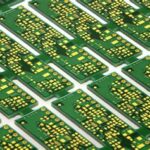
PCB panelization is the process of grouping multiple printed circuit board (PCB) designs onto a single panel for manufacturing. This technique is widely used in the electronics industry to reduce production costs, increase efficiency, and streamline the assembly process. By panelizing PCBs, manufacturers can produce a larger number of boards in a single run, minimizing setup time and material waste.
When it comes to panelizing round-shaped PCBs, there are unique challenges and considerations that must be addressed to ensure a successful manufacturing process. This article will provide a comprehensive guide on how to effectively panelize round-shaped PCBs, covering various aspects such as design considerations, panelization methods, and best practices.
Understanding Round-Shaped PCBs
Round-shaped PCBs are commonly used in various applications, such as wearable devices, IoT sensors, and medical equipment. These PCBs offer several advantages over traditional rectangular boards, including:
- Compact size and unique form factor
- Enhanced aesthetic appeal
- Improved mechanical stability in certain applications
- Reduced sharp edges, making them safer to handle
However, the unique geometry of round-shaped PCBs presents challenges during the panelization process. The absence of straight edges and the presence of curved profiles require special attention to ensure proper panelization and successful manufacturing.
Design Considerations for Round-Shaped PCB Panelization
Board Outline and Dimensions
When designing a round-shaped PCB for panelization, it is essential to consider the board outline and dimensions. The diameter of the round PCB should be carefully chosen based on the specific requirements of the application and the manufacturing capabilities of the PCB fabricator.
It is also important to include appropriate clearances and tolerances around the board outline to accommodate the panelization process. These clearances ensure that there is sufficient space between individual boards on the panel, allowing for proper routing and separation during the depaneling stage.
Placement of Components and Connectors
The placement of components and connectors on a round-shaped PCB requires careful planning to ensure optimal panelization. When positioning components, consider the following factors:
- Clearance between components and the board edge
- Orientation of components to facilitate efficient placement and soldering
- Symmetry and balance of component placement to ensure even distribution of weight and heat dissipation
Connectors should be placed strategically to allow for easy access and assembly after the panelization process. It is recommended to position connectors near the edge of the board, ensuring sufficient clearance for mating connectors and cables.
Panelization Methods for Round-Shaped PCBs
There are several methods for panelizing round-shaped PCBs, each with its own advantages and considerations. The choice of panelization method depends on factors such as the board size, quantity, and manufacturing requirements.
Tab Routing
Tab routing involves connecting individual round PCBs with thin tabs or “spokes” that extend from the board edges. These tabs are typically made from the same material as the PCB substrate and are designed to be easily broken or cut during the depaneling process.
| Advantages | Disadvantages |
|---|---|
| Simple and cost-effective | Limited mechanical strength of tabs |
| Easy to depanel | Potential for damage during depaneling |
| Suitable for small to medium quantities | Not ideal for high-volume production |
V-Scoring
V-scoring is a panelization method that involves creating V-shaped grooves along the perimeter of each round PCB. These grooves are partially cut through the PCB substrate, allowing for easy separation of individual boards after the manufacturing process.
| Advantages | Disadvantages |
|---|---|
| Provides clean and precise board separation | Requires specialized tooling for V-scoring |
| Minimal material waste | Limited to certain PCB thicknesses |
| Suitable for high-volume production | Higher tooling costs compared to tab routing |
Perforated Breakaway
Perforated breakaway panelization involves creating a series of small, closely spaced holes along the perimeter of each round PCB. These perforations allow for easy separation of individual boards by breaking along the perforated lines.
| Advantages | Disadvantages |
|---|---|
| Easy to separate boards | Potential for rough edges after breaking |
| Suitable for various board thicknesses | Increased material waste compared to other methods |
| Cost-effective for small to medium quantities | Not suitable for high-density designs |

Panelization Design Tips and Best Practices
To ensure successful panelization of round-shaped PCBs, consider the following tips and best practices:
-
Maintain consistent board spacing: Ensure that the spacing between individual boards on the panel is consistent and sufficient to accommodate the panelization method chosen.
-
Include fiducial markers: Place fiducial markers on the panel to assist with accurate placement and alignment during the assembly process.
-
Consider panel orientation: Orient the round PCBs on the panel in a way that optimizes material usage and minimizes waste.
-
Use panelization software: Utilize dedicated panelization software tools to automate the process of arranging and optimizing the placement of round PCBs on the panel.
-
Collaborate with your PCB fabricator: Work closely with your PCB fabricator to discuss panelization requirements, design constraints, and any specific guidelines they may have.
Frequently Asked Questions (FAQ)
-
What is the minimum spacing required between round PCBs on a panel?
The minimum spacing between round PCBs on a panel depends on the panelization method used and the specific requirements of the PCB fabricator. Typically, a spacing of 2-3 mm is recommended, but it is best to consult with your fabricator for their specific guidelines. -
Can I panelize round PCBs of different sizes on the same panel?
Yes, it is possible to panelize round PCBs of different sizes on the same panel. However, it is important to ensure that the panelization design accommodates the various sizes and that the spacing between boards is consistent and appropriate for the chosen panelization method. -
How do I choose the best panelization method for my round-shaped PCBs?
The choice of panelization method depends on several factors, including the board size, quantity, and manufacturing requirements. Tab routing is suitable for small to medium quantities and is cost-effective, while V-scoring is ideal for high-volume production and provides clean board separation. Perforated breakaway is a cost-effective option for small to medium quantities but may result in rough edges after breaking. -
Can I panelize round PCBs with different thicknesses on the same panel?
It is generally not recommended to panelize round PCBs with different thicknesses on the same panel. Different board thicknesses may require different panelization methods and can complicate the manufacturing process. It is best to panelize PCBs of the same thickness to ensure consistent results and minimize potential issues. -
How can I optimize material usage when panelizing round PCBs?
To optimize material usage when panelizing round PCBs, consider the following strategies: - Arrange the boards on the panel in a way that minimizes waste and maximizes the number of boards per panel.
- Use panelization software tools to automate the placement and optimization of round PCBs on the panel.
- Collaborate with your PCB fabricator to discuss optimal panel sizes and orientations that align with their manufacturing capabilities.
Conclusion
Panelizing round-shaped PCBs presents unique challenges compared to traditional rectangular boards. By understanding the design considerations, panelization methods, and best practices outlined in this article, you can effectively panelize your round-shaped PCBs and ensure a successful manufacturing process.
Remember to consider factors such as board outline and dimensions, component placement, and the choice of panelization method based on your specific requirements. Collaborating closely with your PCB fabricator and leveraging panelization software tools can further streamline the process and optimize results.
By following the guidelines and tips provided, you can efficiently panelize your round-shaped PCBs, reduce manufacturing costs, and achieve high-quality results for your electronics projects.

