Introduction
In the realm of high-speed digital circuit design, crosstalk has emerged as a significant challenge that can severely impact signal integrity and overall system performance. As data rates continue to increase and traces become more densely packed, the potential for electromagnetic interference between adjacent signal paths amplifies, leading to crosstalk issues. Crosstalk can introduce noise, signal distortion, and data errors, ultimately compromising the reliability and functionality of electronic systems.
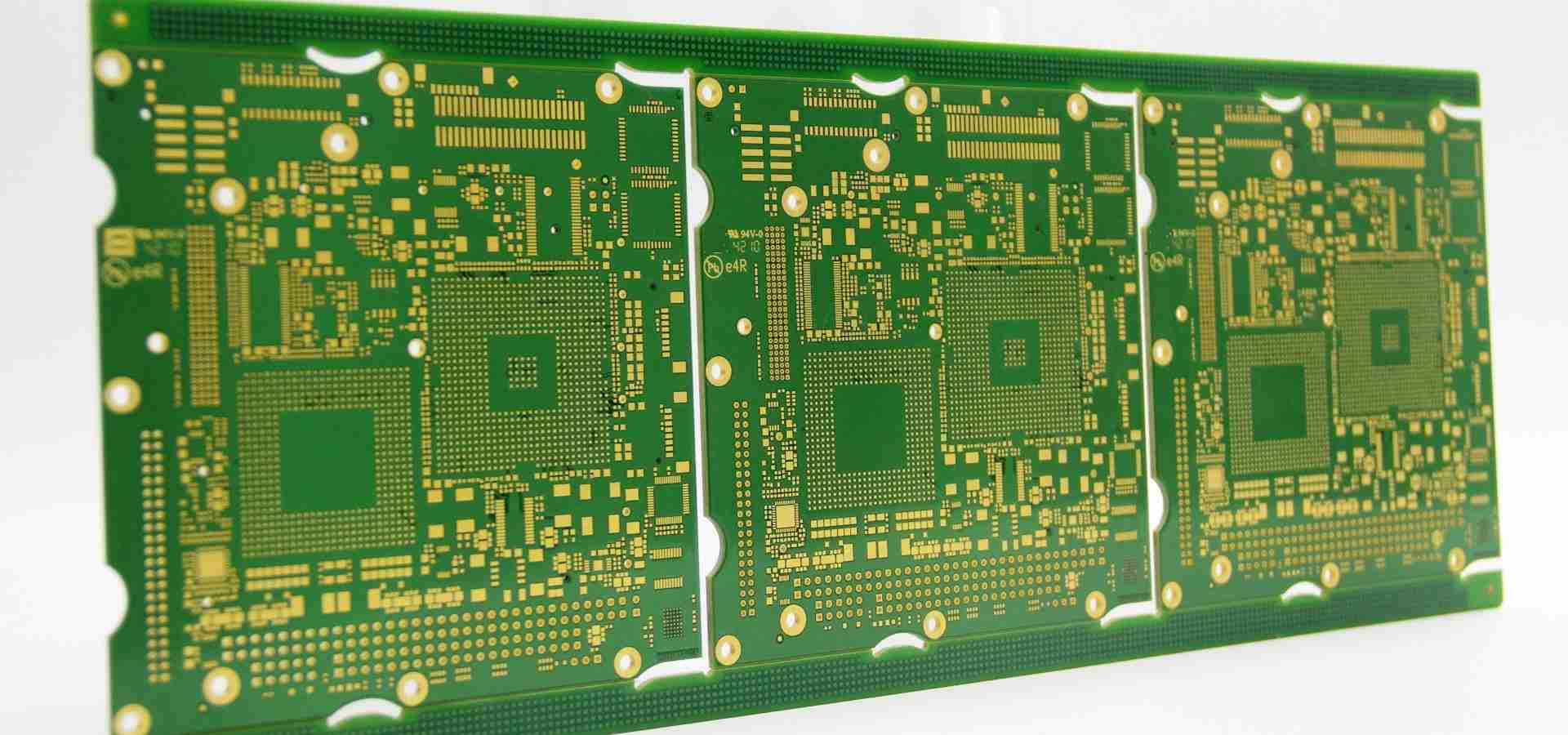
This comprehensive article delves into the analysis and control of crosstalk in high-speed printed circuit board (PCB) design, providing valuable insights and practical strategies to mitigate its effects. We will explore the fundamental principles of crosstalk, its various modes, and the factors that influence its manifestation. Additionally, we will examine advanced techniques for crosstalk analysis and simulation, as well as effective design methodologies and layout practices to minimize crosstalk in high-speed PCB designs.
What is Crosstalk?
Crosstalk refers to the unintended coupling of electromagnetic energy between adjacent signal conductors, such as traces, vias, or cables. This coupling can occur through capacitive, inductive, or conductive mechanisms, resulting in the transfer of noise or signal distortion from one signal path to another. Crosstalk is particularly problematic in high-speed digital systems, where the rapid switching of signals and the close proximity of traces can exacerbate its effects.
Capacitive Crosstalk
Capacitive crosstalk occurs due to the capacitive coupling between adjacent signal traces or conductors. When a signal transitions on one trace, it creates an electric field that induces a voltage on nearby traces, causing unwanted signal coupling. This type of crosstalk is particularly prominent at higher frequencies and shorter trace separations.
Inductive Crosstalk
Inductive crosstalk arises from the magnetic coupling between adjacent signal traces or conductors. When a current flows through a trace, it generates a magnetic field that can induce a voltage in nearby traces, leading to crosstalk. This type of crosstalk is more significant at lower frequencies and with longer parallel trace lengths.
Conductive Crosstalk
Conductive crosstalk occurs when there is a direct conductive path between signal traces or conductors, allowing currents to flow from one trace to another. This type of crosstalk is relatively rare in well-designed PCBs but can occur due to manufacturing defects or improper design practices.
Factors Influencing Crosstalk
Several factors can influence the extent and severity of crosstalk in high-speed PCB designs. Understanding these factors is crucial for effective crosstalk analysis and mitigation strategies.
Trace Separation
The physical distance between adjacent signal traces plays a significant role in crosstalk. Closer trace spacing increases the capacitive and inductive coupling between traces, leading to higher levels of crosstalk.
Trace Length and Parallelism
Longer parallel trace lengths increase the opportunity for inductive crosstalk due to the extended magnetic coupling between the traces. Minimizing parallel trace lengths and reducing the degree of parallelism can help mitigate crosstalk.
Signal Rise Time and Data Rate
Signals with faster rise times and higher data rates are more susceptible to crosstalk effects. The rapid transitions of these signals generate stronger electric and magnetic fields, increasing the potential for crosstalk coupling.
Dielectric Properties
The dielectric materials used in the PCB substrate and the surrounding environment can influence crosstalk behavior. Materials with higher dielectric constants generally exhibit increased capacitive coupling, leading to higher levels of crosstalk.
Ground and Power Plane Configurations
The arrangement and design of ground and power planes in a PCB can impact crosstalk performance. Proper plane configurations, such as solid ground planes and power plane segmentation, can help reduce crosstalk by providing a low-impedance return path and shielding against electromagnetic interference.
Crosstalk Analysis and Simulation
Effective crosstalk analysis and simulation techniques are essential for understanding and predicting crosstalk behavior in high-speed PCB designs. These tools and methodologies allow designers to identify potential crosstalk issues early in the design process and implement appropriate mitigation strategies.
Analytical Models
Analytical models, such as the Broadside Coupled Microstrip Line model and the Parallel Plate Waveguide model, provide mathematical frameworks for estimating crosstalk levels based on various design parameters, including trace geometries, material properties, and signal characteristics.
Numerical Simulation Tools
Numerical simulation tools, such as finite element analysis (FEA) and electromagnetic field solvers, offer more comprehensive and accurate crosstalk analysis capabilities. These tools can account for complex geometries, material properties, and boundary conditions, enabling designers to predict crosstalk levels and signal integrity metrics with high precision.
Signal Integrity Analysis
Signal integrity analysis techniques, such as eye diagram simulations and bit error rate (BER) calculations, can be used to evaluate the impact of crosstalk on signal quality and system performance. These analyses provide quantitative measures of signal degradation and help designers determine acceptable crosstalk levels.
Measurement and Validation
Physical measurements and validation techniques, such as time-domain reflectometry (TDR) and vector network analyzer (VNA) measurements, are crucial for verifying crosstalk simulations and validating the effectiveness of crosstalk mitigation strategies in prototypes and final designs.
Crosstalk Mitigation Techniques
Implementing effective crosstalk mitigation techniques is essential for ensuring reliable and robust high-speed PCB designs. These techniques can be applied at various stages of the design process, from layout optimization to material selection and signal termination strategies.
Layout Optimization
Optimizing the PCB layout can significantly reduce crosstalk levels. Techniques such as increasing trace separation, minimizing parallel trace lengths, and implementing guard traces or ground shielding can effectively mitigate crosstalk coupling.
Signal Routing and Topology
Careful signal routing and topology considerations can help minimize crosstalk. Techniques such as differential signaling, serpentine routing, and signal path length matching can improve signal integrity and reduce crosstalk susceptibility.
Material Selection
Selecting appropriate PCB materials with favorable dielectric properties can help control crosstalk levels. Materials with lower dielectric constants and dissipation factors can reduce capacitive coupling and improve signal integrity.
Signal Termination and Conditioning
Proper signal termination and conditioning strategies can mitigate crosstalk effects. Techniques such as AC-coupled termination, series termination, and common-mode filtering can effectively suppress crosstalk noise and improve signal quality.
Shielding and Isolation
Implementing shielding and isolation techniques can effectively reduce crosstalk coupling. Techniques such as using ground or power planes as shielding layers, employing grounded guard traces, and physically isolating high-speed signals can provide effective crosstalk mitigation.
Design Practices and Guidelines
Adhering to industry-standard design practices and guidelines is crucial for minimizing crosstalk in high-speed PCB designs. These practices ensure consistent and reliable performance across various design scenarios and applications.
Design Rules and Constraints
Establishing and adhering to well-defined design rules and constraints is essential for managing crosstalk. These rules may include guidelines for trace separation, differential pair routing, and spacing requirements based on signal frequencies and data rates.
Signal Integrity Budgeting
Signal integrity budgeting involves allocating acceptable noise margins and defining crosstalk limits based on system requirements and performance targets. This approach ensures that crosstalk levels remain within acceptable bounds and do not compromise overall system functionality.
Design Reviews and Verification
Conducting thorough design reviews and verification processes is crucial for identifying and addressing potential crosstalk issues. These reviews should involve cross-functional teams, including signal integrity experts, layout designers, and system architects, to ensure comprehensive analysis and mitigation strategies.
Compliance with Industry Standards
Adhering to industry standards and specifications, such as those defined by organizations like the IPC (Association Connecting Electronics Industries) and IEEE (Institute of Electrical and Electronics Engineers), can help ensure compliance with best practices for crosstalk control and signal integrity management.
Frequently Asked Questions (FAQ)
- What is the difference between crosstalk and EMI (Electromagnetic Interference)? Crosstalk and EMI are related but distinct phenomena. Crosstalk refers to the unintended coupling of electromagnetic energy between adjacent signal conductors within a system, while EMI refers to the interference caused by external electromagnetic sources, such as nearby electronic devices or environmental factors.
- Is crosstalk more problematic for differential or single-ended signals? Crosstalk is generally less problematic for differential signals compared to single-ended signals. Differential signaling offers inherent noise rejection capabilities, reducing the impact of crosstalk coupling on the signal. However, crosstalk can still affect differential signals, especially if the coupling is asymmetric or if the crosstalk levels are excessive.
- Can crosstalk be eliminated completely in high-speed PCB designs? While it is impossible to eliminate crosstalk completely in high-speed PCB designs, it is possible to mitigate its effects to acceptable levels through careful design practices and crosstalk mitigation techniques. The goal is to manage crosstalk within the specified signal integrity budgets and performance requirements of the system.
- How does the PCB stackup design influence crosstalk? The PCB stackup design, which includes the arrangement and properties of the various layers (signal, ground, and power planes), can significantly impact crosstalk levels. Proper stackup design, such as incorporating solid ground planes, power plane segmentation, and optimized dielectric materials, can help reduce crosstalk coupling and improve signal integrity.
- What are the trade-offs between crosstalk mitigation and other design considerations? While crosstalk mitigation is crucial for high-speed PCB designs, it may sometimes conflict with other design considerations, such as component density, routing complexity, or cost constraints. Designers must carefully balance crosstalk mitigation strategies with other design requirements to achieve an optimal solution that meets all performance and functional requirements.


