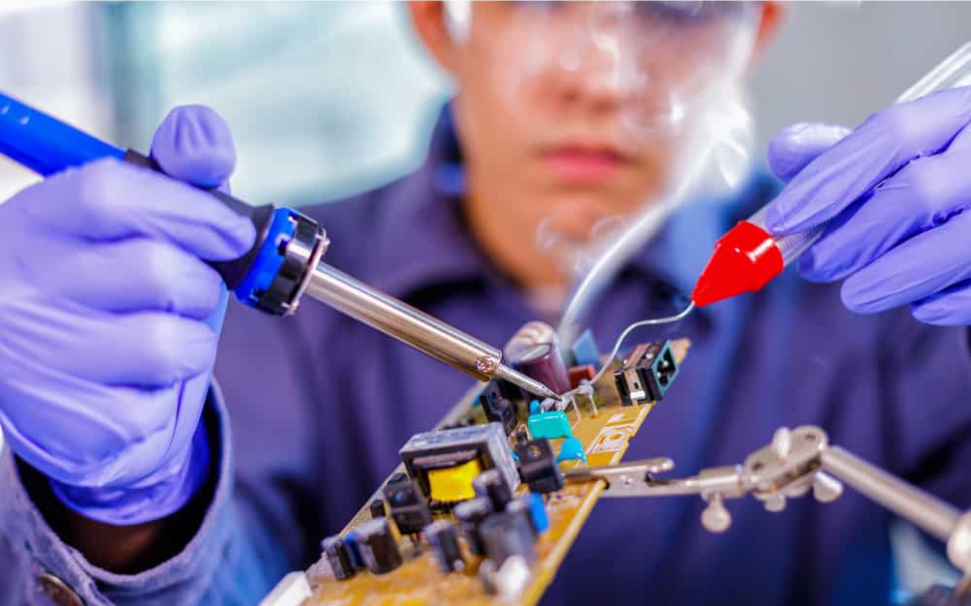
1. Cold Solder Joints
Cold solder joints are one of the most common soldering problems encountered in PCB assembly. They occur when the solder does not melt completely or the joint area is not heated sufficiently during the soldering process. This results in a weak, brittle connection that can lead to intermittent or complete circuit failure over time.
Causes of cold solder joints:
- Insufficient heat transfer to the joint area
- Improper soldering iron temperature
- Oxidized or contaminated surfaces
- Inadequate flux application
- Hurried or rushed soldering process
Consequences of cold solder joints:
- Intermittent connectivity issues
- High resistance in the circuit
- Premature joint failure
- Potential fire hazards due to overheating
Prevention and Remedies:
- Use a properly tinned and high-quality soldering iron with the right tip size and temperature
- Ensure proper flux application and surface preparation
- Allow sufficient heating time for the solder to melt and flow smoothly
- Inspect the joints visually and perform continuity tests
2. Solder Bridges
Solder bridges occur when excess solder creates an unintended electrical connection between adjacent pads, traces, or components on the PCB. This can lead to short circuits, potentially causing damage to the board or connected devices.
Causes of solder bridges:
- Excessive solder application
- Inadequate solder wick or removal techniques
- Improper component placement or spacing
- Contamination or flux residue
Consequences of solder bridges:
- Short circuits and potential component damage
- Unpredictable circuit behavior
- Overheating and potential fire hazards
Prevention and Remedies:
- Use appropriate soldering techniques and solder amount
- Carefully inspect the board during and after soldering
- Utilize solder wick, solder sucker, or desoldering braid to remove excess solder
- Clean the board thoroughly after soldering to remove flux residue
3. Tombstoning
Tombstoning is a phenomenon where one end of a surface-mount component (SMD) becomes unsoldered, causing it to stand up vertically on the board. This issue can be particularly problematic with lightweight or asymmetrical components.
Causes of tombstoning:
- Uneven heating or cooling rates during reflow soldering
- Insufficient solder paste volume or distribution
- Improper pad design or component positioning
- Component weight or size mismatch
Consequences of tombstoning:
- Intermittent or complete loss of electrical connection
- Potential short circuits or damage to adjacent components
- Increased risk of board failure
Prevention and Remedies:
- Optimize the reflow soldering profile for even heating and cooling
- Ensure proper solder paste volume and distribution
- Review pad design and component positioning guidelines
- Consider using adhesives or fixtures to secure components during reflow
4. Dry Joints
Dry joints, also known as insufficient wetting, occur when the solder does not adequately bond with the metal surfaces being joined. This can result in a weak, unreliable connection prone to failure.
Causes of dry joints:
- Oxidized or contaminated surfaces
- Insufficient flux application
- Improper soldering temperature
- Inadequate heating or dwell time
Consequences of dry joints:
- High resistance in the circuit
- Intermittent connectivity issues
- Premature joint failure
- Potential overheating and fire hazards
Prevention and Remedies:
- Ensure proper surface preparation and cleaning
- Apply adequate flux to promote wetting and oxide removal
- Use the correct soldering temperature and heating duration
- Inspect joints visually and perform continuity tests
5. Solder Balling
Solder balling is a phenomenon where the molten solder forms into small, spherical balls instead of flowing smoothly onto the joint surfaces. This can lead to poor electrical connections and potential short circuits.
Causes of solder balling:
- Contaminated or oxidized surfaces
- Insufficient flux application
- Improper soldering temperature or dwell time
- Incompatible solder alloy or flux compositions
Consequences of solder balling:
- Unreliable or intermittent electrical connections
- Potential short circuits or bridging
- Increased risk of component or board failure
Prevention and Remedies:
- Ensure proper surface cleaning and preparation
- Apply adequate flux to promote wetting
- Optimize soldering temperature and dwell time
- Use compatible solder alloy and flux combinations
- Remove solder balls using desoldering tools or braid
6. Lifted Pads
Lifted pads occur when the copper pad on the PCB becomes detached from the board substrate, resulting in a loss of electrical connection. This issue can be caused by excessive heat, physical stress, or improper board construction.
Causes of lifted pads:
- Excessive soldering heat or dwell time
- Mechanical stress or impact during assembly or handling
- Poor board design or manufacturing defects
Consequences of lifted pads:
- Complete loss of electrical connection
- Potential component or trace damage
- Increased risk of board failure
Prevention and Remedies:
- Use appropriate soldering techniques and temperature settings
- Handle the boards with care during assembly and transportation
- Review board design and manufacturing processes
- Consider pad reinforcement or alternative pad designs for critical connections
7. Flux Residue
Flux residue refers to the remnants of flux that remain on the PCB after the soldering process. If not properly removed, these residues can cause various issues, such as short circuits, corrosion, or degradation of electrical performance.
Causes of flux residue buildup:
- Insufficient cleaning or rinsing after soldering
- Use of no-clean or poorly activated flux formulations
- Inadequate cleaning agent or process
- Trapped residues in tight spaces or under components
Consequences of flux residue:
- Potential short circuits or leakage currents
- Corrosion of metallic surfaces and components
- Degradation of insulation resistance and electrical performance
- Cosmetic issues and reduced board reliability
Prevention and Remedies:
- Use appropriate flux formulations and cleaning agents
- Implement thorough cleaning processes after soldering
- Consider board design modifications to facilitate cleaning access
- Inspect and test boards for residue after cleaning
8. Component Overheating
Component overheating can occur when excessive heat is applied during the soldering process, potentially damaging sensitive electronic components or the PCB itself.
Causes of component overheating:
- Improper soldering iron temperature or dwell time
- Inadequate heat sinking or thermal management
- Insufficient cooling or extended reflow cycles
Consequences of component overheating:
- Permanent damage to sensitive components or PCB materials
- Delamination or warping of the board substrate
- Degradation of component performance or lifespan
- Increased risk of board failure or safety hazards
Prevention and Remedies:
- Use appropriate soldering temperatures and techniques
- Employ heat sinks or thermal management strategies for sensitive components
- Optimize reflow soldering profiles and cooling rates
- Monitor component temperatures during assembly
- Replace damaged components and inspect boards after overheating incidents
9. Solder Mask Damage
The solder mask is a protective layer applied to the PCB surface to prevent solder from bridging between conductors and to provide insulation. Damage to the solder mask can compromise the board’s electrical and mechanical integrity.
Causes of solder mask damage:
- Excessive heat during soldering or rework
- Mechanical abrasion or impact
- Chemical exposure or incompatibility
- UV light or moisture degradation
Consequences of solder mask damage:
- Potential short circuits or current leakage
- Reduced insulation resistance
- Corrosion or degradation of exposed copper traces
- Cosmetic issues and reduced board reliability
Prevention and Remedies:
- Use appropriate soldering techniques and temperatures
- Handle boards with care during assembly and transportation
- Protect boards from chemical exposure or harsh environments
- Consider conformal coating or alternative solder mask materials for harsh conditions
10. Missing or Misaligned Components
Missing or misaligned components can occur during the assembly process, leading to incomplete or malfunctioning circuits on the PCB.
Causes of missing or misaligned components:
- Improper component placement or handling
- Faulty pick-and-place equipment or programming
- Inadequate component retention or adhesive
- Vibration or physical disturbance during assembly
Consequences of missing or misaligned components:
- Complete or partial circuit failure
- Potential short circuits or bridging
- Reduced reliability and performance
- Increased risk of board rework or replacement
Prevention and Remedies:
- Implement robust component handling and placement procedures
- Calibrate and maintain pick-and-place equipment regularly
- Use component retention strategies (e.g., adhesives, fixtures)
- Minimize vibration and physical disturbances during assembly
- Implement quality control measures to detect and correct issues
11. Reverse Polarity
Reverse polarity refers to the incorrect orientation or connection of polarized components, such as diodes, electrolytic capacitors, or integrated circuits (ICs), on the PCB.
Causes of reverse polarity:
- Incorrect component placement or orientation
- Inadequate polarity marking or identification
- Human error during manual assembly
- Faulty programming or component library data
Consequences of reverse polarity:
- Component damage or failure
- Unpredictable circuit behavior
- Potential safety hazards (e.g., overheating, fire)
- Increased risk of board rework or replacement
Prevention and Remedies:
- Implement clear polarity markings and component orientation guidelines
- Utilize automated component placement and verification systems
- Conduct thorough visual inspections and electrical testing
- Maintain accurate component library data and programming
- Train personnel on proper component handling and assembly procedures
12. Electrostatic Discharge (ESD) Damage
Electrostatic discharge (ESD) can potentially damage sensitive electronic components on the PCB, leading to performance degradation or complete failure.
Causes of ESD damage:
- Static electricity buildup during handling or assembly
- Inadequate ESD protection measures
- Improper grounding or shielding of equipment and workstations
- Environmental factors (e.g., low humidity, synthetic materials)
Consequences of ESD damage:
- Permanent or latent component damage
- Intermittent or complete circuit failure
- Reduced component lifespan and reliability
- Increased risk of board rework or replacement
Prevention and Remedies:
- Implement proper ESD control measures (e.g., grounding, wrist straps, ionizers)
- Use ESD-safe materials and workstations
- Handle components and boards with care in controlled environments
- Conduct ESD testing and compliance checks regularly
- Train personnel on ESD awareness and prevention techniques
FQA (Frequently Asked Questions)
1. What is the most common cause of cold solder joints?
The most common cause of cold solder joints is insufficient heat transfer to the joint area, often due to an improper soldering iron temperature or hurried soldering process. Oxidized or contaminated surfaces and inadequate flux application can also contribute to cold solder joints.
2. How can I prevent solder bridges during PCB assembly?
To prevent solder bridges, it’s crucial to use appropriate soldering techniques and solder amount. Carefully inspect the board during and after soldering, and utilize solder wick, solder sucker, or desoldering braid to remove excess solder. Additionally, thoroughly clean the board after soldering to remove flux residue.
3. What are the consequences of tombstoning in surface-mount components?
Tombstoning can lead to intermittent or complete loss of electrical connection, potential short circuits or damage to adjacent components, and an increased risk of board failure. It can be particularly problematic for lightweight or asymmetrical components.
4. How can I identify and address dry joints during soldering?
Dry joints, or insufficient wetting, can be identified by visual inspection and continuity testing. To prevent dry joints, ensure proper surface preparation and cleaning, apply adequate flux, use the correct soldering temperature and heating duration, and inspect joints thoroughly.
5. What are the potential causes of solder balling, and how can it be prevented?
Solder balling can be caused by contaminated or oxidized surfaces, insufficient flux application, improper soldering temperature or dwell time, and incompatible solder alloy or flux compositions. To prevent solder balling, ensure proper surface cleaning and preparation, apply adequate flux, optimize soldering parameters, and use compatible materials.


