Introduction
In the world of electronics, printed circuit boards (PCBs) are the backbone of almost every electronic device. Whether it’s a simple LED circuit or a complex microcontroller-based system, PCBs provide the necessary interconnections between electronic components. While manufacturing PCBs professionally can be expensive, there are cost-effective methods for hobbyists and enthusiasts to create their own PCBs at home. One of these methods is the toner transfer etching process, which utilizes readily available materials and tools.
The toner transfer method is a popular DIY technique for etching PCBs. It involves transferring a printed circuit design onto a copper-clad board using a laser printer or photocopier, and then etching away the unwanted copper, leaving behind the desired circuit pattern. This method is relatively inexpensive, easy to set up, and produces high-quality results.
In this comprehensive article, we will guide you through the nine essential steps to etch a PCB using the toner transfer method. We will cover everything from preparing the circuit design to the final cleaning and inspection process. Whether you’re a hobbyist, student, or an electronics enthusiast, this article will equip you with the knowledge and techniques to create your own custom PCBs at home.
Step 1: Prepare the Circuit Design
H3: Create or Obtain a Circuit Design
The first step in the toner transfer etching process is to obtain or create a circuit design. There are various software tools available for designing PCBs, such as Eagle, KiCad, and Fritzing. These software packages allow you to create schematic diagrams and layout the circuit components on a virtual PCB.
If you’re new to circuit design, it’s recommended to start with simple projects or use pre-existing designs available online. Many websites offer free PCB design files for various electronic projects, which can be downloaded and used as a starting point.
H3: Print the Circuit Design
Once you have your circuit design ready, the next step is to print it onto a glossy paper or transparency film using a laser printer or photocopier. Inkjet printers are not suitable for this process as the ink can smear or run during the etching process.
It’s important to ensure that the print quality is high, with sharp and crisp lines. Adjust the printer settings to achieve the best possible contrast and resolution. Additionally, make sure to print the design at the actual size (1:1 scale) to avoid any scaling issues during the transfer process.
Step 2: Prepare the Copper-Clad Board
H3: Choose the Appropriate Copper-Clad Board
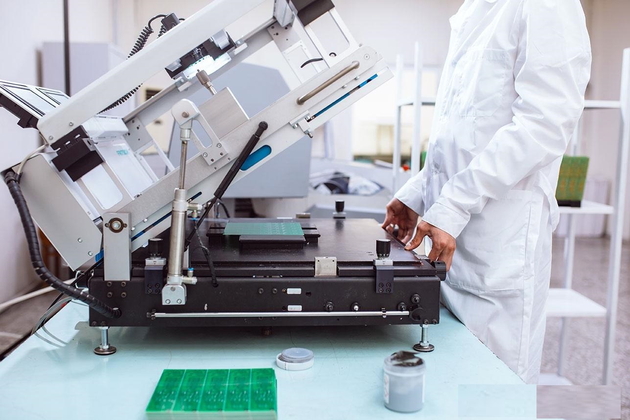
Copper-clad boards are available in various materials, such as FR-4 (fiberglass reinforced epoxy), phenolic, and other composite materials. For most hobbyist and prototyping purposes, FR-4 boards are the most common and widely used option due to their durability and affordability.
When selecting a copper-clad board, consider the desired thickness, copper weight (oz/ft²), and the number of layers (single-sided or double-sided). The thickness and copper weight will depend on the specific requirements of your project and the components you plan to use.
H3: Clean the Copper-Clad Board
Before proceeding with the toner transfer process, it’s crucial to clean the copper-clad board thoroughly. Any residual oils, dirt, or contaminants on the surface can interfere with the toner transfer and etching process, leading to poor results.
Use a degreaser or isopropyl alcohol and a clean, lint-free cloth to wipe down the copper surface. Ensure that the surface is free of any fingerprints or smudges, as these can also affect the toner transfer.
Step 3: Transfer the Circuit Design
H3: Prepare the Toner Transfer Setup
For the toner transfer process, you will need a few essential items:
- A flat, sturdy surface (e.g., a piece of plywood or a laminated surface)
- A heavy-duty laminator or a clothing iron
- Parchment paper or glossy magazine pages
Arrange the toner transfer setup by placing the copper-clad board on the flat surface, followed by the printed circuit design (toner side down), and finally the parchment paper or glossy magazine pages on top.
H3: Transfer the Toner to the Copper-Clad Board
If you’re using a laminator, follow the manufacturer’s instructions to set the appropriate temperature and feed the setup through the laminator. The heat and pressure will transfer the toner from the printed design onto the copper surface.
If you’re using a clothing iron, ensure that it’s set to the highest heat setting (without steam). Place the setup on the flat surface and press the iron firmly onto the parchment paper or glossy magazine pages. Move the iron slowly and evenly across the entire surface, applying consistent pressure for a few minutes.
After the transfer process is complete, carefully peel off the parchment paper or glossy magazine pages. If the transfer was successful, you should see the circuit design transferred onto the copper surface in toner.
Step 4: Prepare the Etching Solution
H3: Choose the Etching Solution
There are several etching solutions available for etching copper-clad boards, each with its own advantages and disadvantages. Some common etching solutions include:
- Ferric chloride (FeCl₃) solution
- Ammonium persulfate (NH₄)₂S₂O₈ solution
- Sodium persulfate (Na₂S₂O₈) solution
- Hydrochloric acid (HCl) and hydrogen peroxide (H₂O₂) mixture
Ferric chloride is one of the most widely used and readily available etching solutions for hobbyists. It is relatively inexpensive, easy to handle, and provides consistent etching results.
H3: Prepare the Etching Container
Choose a non-metallic container (plastic or glass) that is large enough to accommodate your copper-clad board. The container should be shallow enough to allow the etching solution to cover the entire surface of the board.
Ensure that the container is clean and free from any contaminants that could interfere with the etching process. It’s also recommended to use a separate container for the etching solution to avoid cross-contamination with other chemicals or solutions.
Step 5: Etch the Copper-Clad Board
H3: Immerse the Board in the Etching Solution
Carefully place the copper-clad board with the transferred circuit design into the etching solution. Ensure that the entire surface is submerged and that there are no air bubbles trapped underneath the board.
During the etching process, gently agitate the solution by rocking the container back and forth or using a non-metallic stirring rod. This helps to keep the etching solution fresh and evenly distributed across the board’s surface.
H3: Monitor the Etching Process
The etching process can take anywhere from a few minutes to several hours, depending on the strength of the etching solution, the thickness of the copper, and the desired etch depth.
Periodically check the progress of the etching by carefully removing the board from the solution and inspecting the copper surface. The areas not covered by toner should be etched away, leaving the desired circuit pattern on the board.
Once the etching is complete, carefully remove the board from the solution and rinse it thoroughly with clean water to stop the etching process and remove any residual etching solution.
Step 6: Remove the Toner Transfer
H3: Use a Toner Transfer Removal Solution
After the etching process is complete, the toner transfer must be removed from the copper surface to reveal the final circuit pattern. There are several toner transfer removal solutions available, such as:
- Sodium hydroxide (NaOH) solution
- Trichloroethylene (C₂HCl₃)
- Toner transfer remover (commercial products)
Sodium hydroxide (lye) solution is a common and effective toner transfer removal solution. However, it is highly corrosive and should be handled with extreme caution, following proper safety precautions.
H3: Immerse the Board in the Toner Transfer Removal Solution
Carefully place the etched board into the toner transfer removal solution, ensuring that the entire surface is submerged. Gently agitate the solution or use a soft-bristled brush to assist in the removal process.
Monitor the progress closely, as the toner transfer should begin to lift off the copper surface after a few minutes. Once the toner transfer is completely removed, rinse the board thoroughly with clean water to remove any residual solution.
Step 7: Drill Component Holes
H3: Marking and Drilling Holes
After the etching and toner transfer removal processes are complete, you will need to drill holes in the PCB to accommodate the leads of electronic components.
Use a fine-tipped permanent marker or a PCB marker pen to mark the locations of the holes on the copper surface, following the layout of your circuit design.
Choose the appropriate drill bit size based on the component lead diameters. For most through-hole components, drill bit sizes ranging from 0.6mm to 1.2mm are commonly used.
Secure the PCB on a flat, stable surface and carefully drill the marked holes using a drill press or a handheld drill. Ensure that the drill is perpendicular to the PCB surface to achieve clean, accurate holes.
Step 8: Clean and Inspect the PCB
H3: Remove Any Remaining Residue
After the drilling process, it’s essential to thoroughly clean the PCB to remove any remaining residue or debris from the etching and drilling processes.
Use a soft-bristled brush and a mild cleaning solution, such as isopropyl alcohol or a PCB cleaner, to gently scrub the copper surface and the drilled holes. Rinse the PCB with clean water and dry it thoroughly with a clean, lint-free cloth or compressed air.
H3: Inspect the PCB for Defects
Once the PCB is clean and dry, carefully inspect it for any defects or irregularities. Check for any remaining toner transfer, scratches, or any other imperfections that could potentially cause issues during component assembly or circuit operation.
If any defects are found, you may need to repeat the etching or drilling process, or consider starting over with a new copper-clad board.
Step 9: Prepare for Component Assembly
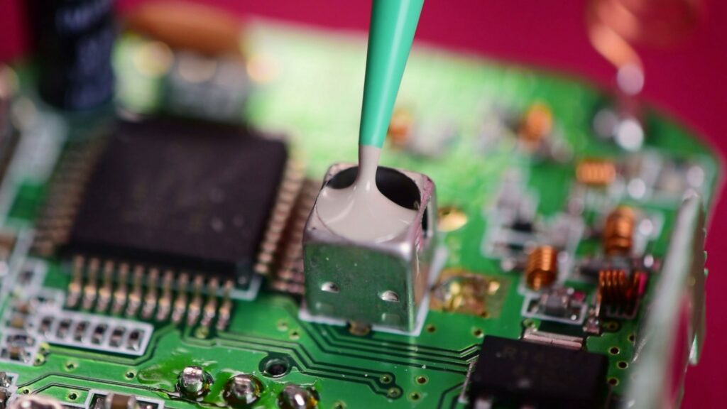
H3: Apply Solder Mask (Optional)
Applying a solder mask is an optional step that can help protect the copper traces and prevent accidental shorts during the component assembly process.
Solder masks are available in various forms, such as liquid or dry film photoimageable solder masks. These masks are applied to the PCB surface, covering the copper traces while leaving the component pads and drilled holes exposed.
Follow the manufacturer’s instructions for applying and curing the solder mask, ensuring proper coverage and adhesion to the PCB.
H3: Prepare for Component Assembly
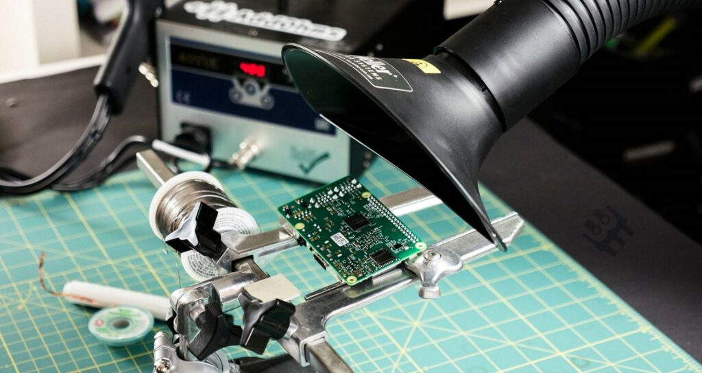
Once the PCB is ready, you can proceed with the component assembly process. This typically involves soldering the electronic components onto the PCB, following the circuit design and layout.
Ensure that you have all the necessary components, tools, and equipment ready, such as a soldering iron, solder, flux, and any other required accessories. Follow proper soldering techniques and safety guidelines to ensure a successful component assembly process.
Frequently Asked Questions (FAQs)
1. Can I use an inkjet printer for the toner transfer process?
No, inkjet printers are not suitable for the toner transfer process. The ink used in inkjet printers can smear or run during the etching process, resulting in poor transfer quality and inaccurate circuit patterns. It’s essential to use a laser printer or photocopier for the toner transfer process.
2. How long does the etching process take?
The etching process duration can vary depending on several factors, such as the strength of the etching solution, the thickness of the copper, and the desired etch depth. Typically, the etching process can take anywhere from a few minutes to several hours. It’s essential to monitor the progress regularly and remove the board from the etching solution once the desired etch depth is achieved.
3. Can I reuse the etching solution?
Yes, it is possible to reuse the etching solution, but its effectiveness will gradually decrease over time. The etching solution becomes less potent as it reacts with the copper and accumulates contaminants. It’s recommended to replace the etching solution periodically or when it becomes visibly discolored or ineffective.
4. What safety precautions should I take during the etching process?
When working with etching solutions and chemicals, it’s crucial to take proper safety precautions. Always wear protective equipment such as goggles, gloves, and a lab coat or apron. Ensure adequate ventilation in your workspace and avoid inhaling any fumes or vapors. Additionally, handle all chemicals with care and follow the manufacturer’s instructions and safety guidelines.
5. Can I use the toner transfer method for double-sided PCBs?
Yes, the toner transfer method can be used for creating double-sided PCBs, but it requires an additional step. After etching one side of the board, you will need to transfer and etch the circuit design on the other side as well. Proper alignment and registration of the two sides are crucial for successful double-sided PCB fabrication.


