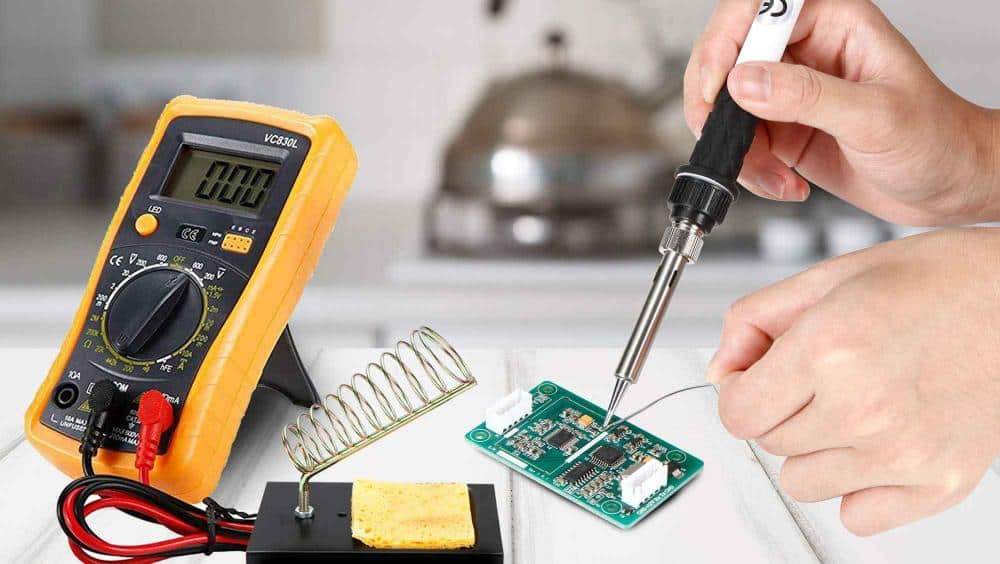
Introduction
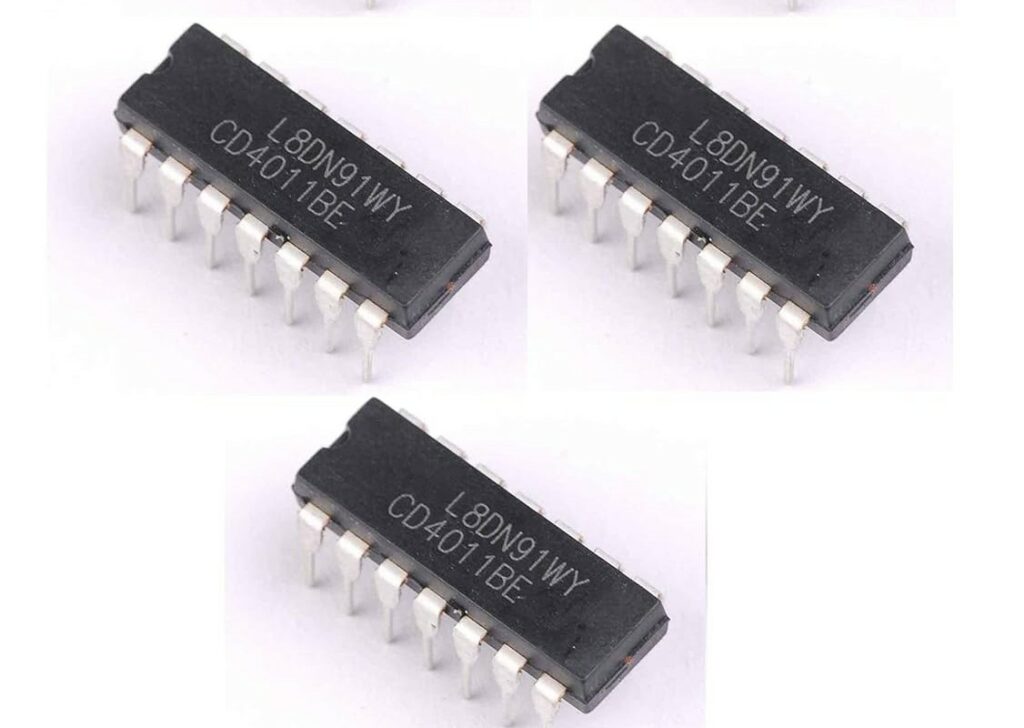
The 4011 IC is a versatile and widely used integrated circuit that belongs to the CMOS (Complementary Metal-Oxide-Semiconductor) family. It is a quad 2-input NAND gate, which means it contains four independent NAND gates within a single IC package. NAND gates are fundamental logic gates used in digital electronics, and their versatility allows them to be used as building blocks for more complex digital circuits.
What is a NAND Gate?
Before delving into the details of the 4011 IC, it is essential to understand the concept of a NAND gate. A NAND gate is a digital logic gate that performs the NAND operation. The NAND operation is a combination of the logical AND and the logical NOT operations.
The truth table for a NAND gate with two inputs (A and B) is as follows:
| Input A | Input B | Output |
|---|---|---|
| 0 | 0 | 1 |
| 0 | 1 | 1 |
| 1 | 0 | 1 |
| 1 | 1 | 0 |
As you can see from the truth table, the output of a NAND gate is LOW (0) only when both inputs are HIGH (1). In all other cases, the output is HIGH (1).
Features of the 4011 IC
The 4011 IC offers several features that make it a popular choice for various digital circuit applications:
- Quad 2-Input NAND Gates: As mentioned earlier, the 4011 IC contains four independent 2-input NAND gates within a single package. This allows for a compact implementation of digital circuits that require multiple NAND gates.
- CMOS Technology: The 4011 IC is fabricated using CMOS technology, which offers several advantages over other technologies, such as low power consumption, high noise immunity, and a wide range of operating voltages.
- Wide Operating Voltage Range: The 4011 IC can operate within a voltage range of 3V to 15V, making it suitable for various applications with different power supply requirements.
- High Input Impedance: The input impedance of the 4011 IC is extremely high, which means it draws minimal current from the driving circuit, reducing the load on the driving circuit and improving overall circuit efficiency.
- Low Output Impedance: The output impedance of the 4011 IC is low, allowing it to drive multiple inputs without significant signal degradation.
- Buffered Outputs: Each NAND gate within the 4011 IC has a buffered output, which means the output can drive a relatively high capacitive load without compromising the signal integrity.
Applications of the 4011 IC
The versatility of the 4011 IC makes it suitable for a wide range of applications in various fields, including:
- Digital Circuit Design: The 4011 IC is widely used in the design of digital circuits, such as combinational logic circuits, sequential logic circuits, and memory circuits.
- Control Systems: The 4011 IC can be used in control systems for various applications, such as industrial automation, robotics, and process control.
- Pulse Generation: The 4011 IC can be configured as an oscillator or pulse generator, making it useful in applications that require precise timing or pulse generation, such as clock circuits or signal processing.
- Interfacing: The 4011 IC can be used as an interface between different digital circuits or systems, allowing for signal level translation or logic level conversion.
- Educational and Prototyping: Due to its simplicity and versatility, the 4011 IC is often used in educational settings to teach digital electronics concepts and in prototyping and experimenting with digital circuits.
Pinout and Internal Structure
To understand the operation of the 4011 IC, it is essential to familiarize yourself with its pinout and internal structure.
Pinout
The 4011 IC is typically packaged in a 14-pin Dual-In-Line Package (DIP) or a Small Outline Integrated Circuit (SOIC) package. The pinout of the 4011 IC is as follows:Copy code
----- +V|1 14|VCC A1|2 13|B4 B1|3 12|A4 Y1|4 11|Y4 GND|5 10|Y3 Y2|6 9|B3 B2|7 8|A3 -----
- Pin 1: +V (Positive Supply Voltage)
- Pin 2: A1 (Input A of NAND Gate 1)
- Pin 3: B1 (Input B of NAND Gate 1)
- Pin 4: Y1 (Output of NAND Gate 1)
- Pin 5: GND (Ground)
- Pin 6: Y2 (Output of NAND Gate 2)
- Pin 7: B2 (Input B of NAND Gate 2)
- Pin 8: A3 (Input A of NAND Gate 3)
- Pin 9: B3 (Input B of NAND Gate 3)
- Pin 10: Y3 (Output of NAND Gate 3)
- Pin 11: Y4 (Output of NAND Gate 4)
- Pin 12: A4 (Input A of NAND Gate 4)
- Pin 13: B4 (Input B of NAND Gate 4)
- Pin 14: VCC (Positive Supply Voltage)
Internal Structure
The internal structure of the 4011 IC consists of four independent NAND gates, each with its own input and output terminals. Each NAND gate is implemented using a combination of CMOS transistors and other components.
The schematic symbol for a single NAND gate within the 4011 IC is as follows:Copy code
+V | | | +---| | | A --| | | |---+ +---| | | | B --| | | | | | +---|---| | | | GND
In this schematic, the inputs A and B are connected to the NAND gate, and the output is represented by the line at the bottom. The power supply connections (+V and GND) are also shown.
Applications and Examples
The 4011 IC can be used in a variety of digital circuits and applications. Here are a few examples:
1. Logic Gates and Combinational Circuits
The 4011 IC can be used to implement various logic gates and combinational circuits by combining its NAND gates in different configurations. For example, an AND gate can be implemented by connecting the output of one NAND gate to the input of another NAND gate and using the second NAND gate’s output as the AND gate output.
2. Oscillators and Pulse Generators
The 4011 IC can be configured as an oscillator or pulse generator by connecting two NAND gates in a specific arrangement, along with external passive components like resistors and capacitors. This configuration can be used to generate clock signals or timing pulses for various applications.
3. Interfacing and Level Shifting
The 4011 IC can be used for interfacing and level shifting between different digital circuits or systems that operate at different voltage levels. By connecting the inputs and outputs of the NAND gates in specific configurations, the 4011 IC can translate signals between different voltage levels, ensuring compatibility between different circuits or systems.
4. Control Systems and Automation
The 4011 IC can be used in control systems and automation applications, where digital logic circuits are required for decision-making, sequencing, or controlling various processes or devices. The NAND gates within the 4011 IC can be combined to implement various logic functions and control algorithms.
5. Educational and Prototyping
Due to its simplicity and versatility, the 4011 IC is often used in educational settings to teach digital electronics concepts and in prototyping and experimenting with digital circuits. Students and hobbyists can use the 4011 IC to build and test various digital circuits, gaining hands-on experience and understanding of digital logic design.
Frequently Asked Questions (FAQ)
- What is the difference between the 4011 IC and other NAND gate ICs like the 7400 or 74LS00?
The 4011 IC is a CMOS (Complementary Metal-Oxide-Semiconductor) integrated circuit, while the 7400 and 74LS00 are TTL (Transistor-Transistor Logic) integrated circuits. CMOS ICs generally have lower power consumption, higher noise immunity, and a wider operating voltage range compared to TTL ICs. Additionally, the 4011 IC contains four independent NAND gates, while the 7400 and 74LS00 contain four NAND gates with shared inputs.
- Can the 4011 IC be used for analog applications?
No, the 4011 IC is a digital integrated circuit designed for digital logic applications. It is not suitable for analog applications as it operates in a binary fashion, providing only two output states (HIGH or LOW).
- What is the maximum operating frequency of the 4011 IC?
The maximum operating frequency of the 4011 IC depends on various factors, such as the supply voltage, load capacitance, and temperature. Typically, the 4011 IC can operate at frequencies up to several megahertz (MHz) range.
- Can the 4011 IC be used as an inverter?
Yes, the 4011 IC can be used as an inverter by connecting one of its NAND gate inputs to a constant logic level (either HIGH or LOW) and using the other input as the signal input. The output of the NAND gate will then be the inverted version of the input signal.
- How do I properly handle and store the 4011 IC?
Like most integrated circuits, the 4011 IC should be handled with care to prevent electrostatic discharge (ESD) damage. It is recommended to use proper ESD-safe handling techniques, such as wearing an anti-static wrist strap and working on an anti-static mat. Additionally, the 4011 IC should be stored in an ESD-safe container or packaging when not in use.


