PCB
-
What is Thermoelectric Copper Base PCB ?
Posted by
–
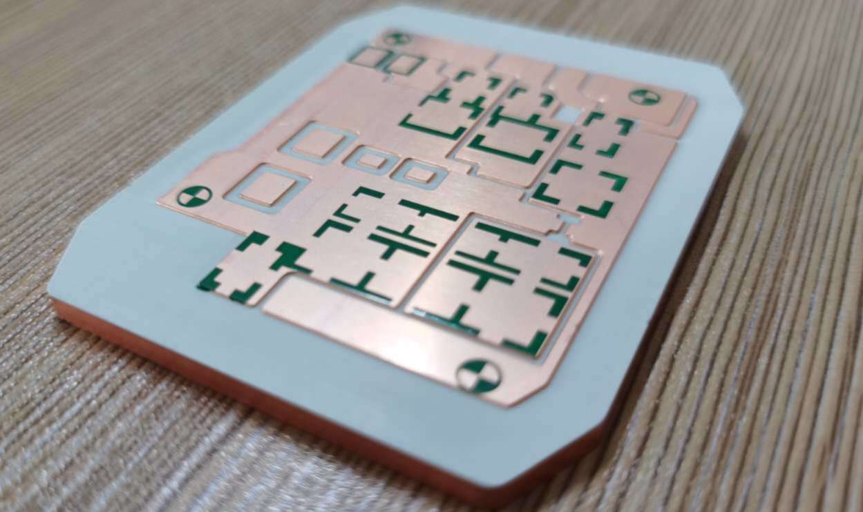
Read more: What is Thermoelectric Copper Base PCB ?Thermoelectric modules (TEMs) use the Peltier effect to provide precise heating or cooling capabilities without liquids or gases. The active thermoelectric elements are mounted between two substrates that transfer heat – typically a metal base and a printed circuit board. The substrate combination is key for managing the thermal load. … Read more
-
How Thick Gold Can be Plated on a PCB?
Posted by
–
 Read more: How Thick Gold Can be Plated on a PCB?
Gold plating provides a highly conductive, corrosion resistant surface finish for printed circuit boards. However, thick gold plating is expensive, so PCB designers must use it judiciously. This article examines how thick gold can be plated on a PCB based on process limitations, reliability factors, use cases and cost considerations. … Read more
-
What Does THT Mean in PCB?
Posted by
–
 Read more: What Does THT Mean in PCB?
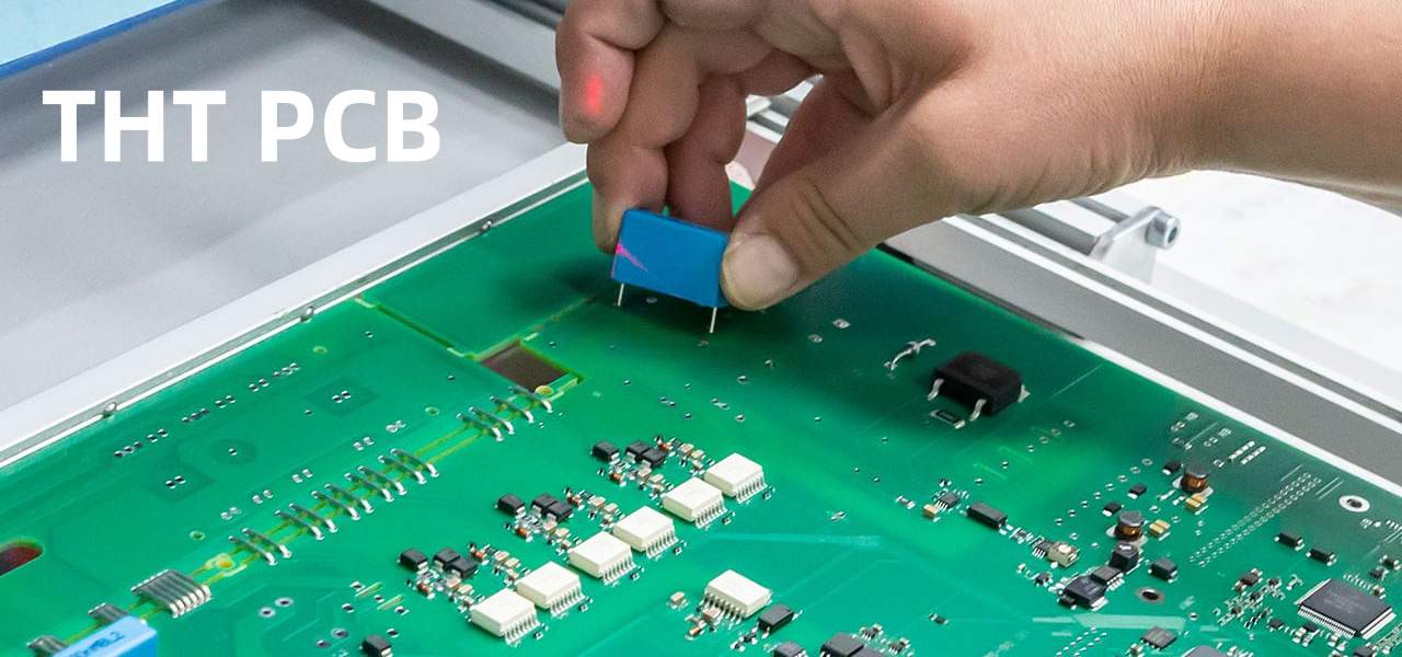
THT stands for Through-Hole Technology when referring to PCBs. It represents the mounting and interconnecting of electronic components using leads passed through holes drilled in the circuit board. THT contrast with SMT (Surface Mount Technology) where components are directly soldered onto surface pads without leads passing through the board. This … Read more
-
What iS TKL PCB ?
Posted by
–
 Read more: What iS TKL PCB ?
TKL PCBs refer to the printed circuit boards used in tenkeyless mechanical keyboards. Tenkeyless or TKL keyboards provide a compact layout without the number pad section for more ergonomic positioning during gaming or regular typing. This article will provide a detailed look at TKL PCB characteristics, layouts, components, build process, … Read more
-
What is PCB Tombstone?
Posted by
–
 Read more: What is PCB Tombstone?
During soldering of surface mount components on printed circuit boards, a defect known as “tombstoning” sometimes occurs. This involves components standing upright on one end rather than lying flat flush to the board after soldering. Tombstoned parts often completely fail from lack of soldering or induce shorts, rendering the PCB … Read more
-
PCB Trace Resistance Calculator (with Formulas)
Posted by
–
 Read more: PCB Trace Resistance Calculator (with Formulas)
The resistance of printed circuit board (PCB) traces impacts current capacity, voltage drop, power dissipation, and signal quality. Accurately calculating trace resistance is important during PCB design to ensure proper performance. This guide provides designers useful formulas and an easy-to-use trace resistance calculator to determine resistance based on trace dimensions … Read more
-
How Do You Calculate Trace Width?
Posted by
–
 Read more: How Do You Calculate Trace Width?
Determining the correct trace width is a critical aspect of printed circuit board (PCB) design. Trace width has a major impact on current carrying capacity, voltage drop, thermal performance and signal integrity. Insufficient trace widths can cause overheating or failure of the circuit. Excessively large traces waste valuable board space … Read more
-
 Read more: PCB Trace Width vs. Current Table for High Power Designs
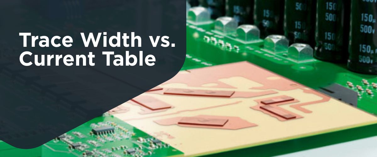
Printed circuit boards (PCBs) provide the interconnect foundation for electronics. A key role of the PCB is safely routing power throughout the system. For high power applications, factors like trace width must be carefully designed to handle required currents. Trace width has a major impact on current capacity. Wider traces … Read more
-
What Does a Transistor Do on a Circuit Board?
Posted by
–
 Read more: What Does a Transistor Do on a Circuit Board?
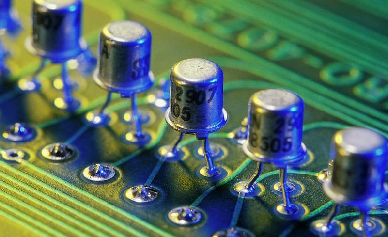
Printed circuit boards are the foundation of electronics, housing components like integrated circuits, resistors, and capacitors. One fundamental component found across nearly every circuit board is the transistor. But what exactly does a transistor do? Transistors enable key functions like amplification, switching, and voltage conversion that underpin modern electronics. This … Read more
-
 Read more: Transparent PCB: See-Through Circuit Board with High Optical Transmissivity
Printed circuit boards (PCBs) form the backbone of electronics and enable the connection of components into functioning devices. Traditionally, PCB substrates use opaque insulating materials that block light transmission. But new transparent PCB technology is emerging that allows light to pass through the board. Transparent PCBs open exciting possibilities in … Read more
Recent Posts
- Understanding the PCB Burn-in Testing Process in PCB Manufacturing!

- Unlock the Potential of Embedded PCB Assemblies for Improving the Performance of Electronics Devices

- What are the Advantages of Custom Cable Assembly to meet your bespoke needs?

- What are the benefits and limitations of custom PCB boards?

- What are the benefits of Prototype PCB manufacturing and why is it important?

Categories
- 3D Guides 2,663
- Components 4
- Design 22
- Electronics 20
- PCB 125
- SMT 27
Tag Cloud
There’s no content to show here yet.