Signal Integrity in Telecom PCB Design
Signal integrity is a critical factor in telecom PCB design, as it directly impacts the quality and reliability of data transmission. High-speed signals are prone to various issues, such as reflections, crosstalk, and attenuation, which can lead to data corruption and system failures. To ensure optimal signal integrity, designers must consider the following aspects:
Impedance Matching
Impedance matching is essential to minimize signal reflections and ensure efficient power transfer. Designers must carefully select the appropriate trace widths, dielectric materials, and layer stackups to achieve the desired characteristic impedance. Common impedance values for telecom applications include 50Ω for RF signals and 100Ω for differential pairs.
Trace Routing
Proper trace routing is crucial for maintaining signal integrity. Designers should follow best practices, such as:
- Minimizing trace lengths to reduce attenuation and delay
- Avoiding sharp bends and corners to prevent reflections
- Maintaining consistent trace widths and spacing to ensure uniform impedance
- Using diagonal routing to minimize crosstalk between adjacent traces
Via Optimization
Vias are essential for connecting traces between layers, but they can also introduce discontinuities and reflections. To minimize the impact of vias on signal integrity, designers should:
- Use smaller via diameters to reduce capacitance and inductance
- Optimize via placement to minimize stub lengths
- Employ via stitching to reduce the effective via length and improve signal quality
Electromagnetic Compatibility (EMC) Considerations
Telecom PCBs are subject to strict EMC regulations to ensure they do not interfere with other electronic devices and can operate reliably in the presence of electromagnetic interference (EMI). Designers must consider the following EMC aspects:
Shielding
Effective shielding is essential to prevent EMI from affecting sensitive components and circuits. Designers can implement shielding techniques such as:
- Using grounded copper planes to create Faraday cages around sensitive areas
- Incorporating shielding cans or enclosures to isolate high-frequency components
- Applying conductive coatings or gaskets to seal gaps and openings
Grounding and Power Distribution
Proper grounding and power distribution are crucial for minimizing EMI and ensuring stable operation. Designers should:
- Use solid ground planes to provide low-impedance return paths for high-frequency signals
- Implement power and ground plane partitioning to isolate noisy circuits from sensitive ones
- Employ decoupling capacitors to reduce power supply noise and transients
Filtering and Suppression
Filtering and suppression techniques can help mitigate EMI and improve EMC performance. Designers can use:
- LC filters to attenuate high-frequency noise on power and signal lines
- Ferrite beads to suppress common-mode noise and high-frequency transients
- Transient voltage suppressors (TVS) to protect against electrostatic discharge (ESD) and voltage spikes
Thermal Management in Telecom PCB Design
Telecom PCBs often involve high-power components and dense layouts, which can lead to significant heat generation. Effective thermal management is essential to ensure reliable operation and prevent premature component failure. Designers should consider the following thermal management techniques:
Component Placement
Strategic component placement can help distribute heat evenly across the PCB and prevent hot spots. Designers should:
- Place high-power components away from sensitive devices
- Provide adequate spacing between components to allow for efficient heat dissipation
- Locate temperature-sensitive components in cooler areas of the PCB
Thermal Vias and Planes
Thermal vias and planes can help conduct heat away from components and dissipate it into the environment. Designers can:
- Use thermal vias to create low-resistance heat paths between components and ground planes
- Incorporate dedicated thermal planes to spread heat evenly across the PCB
- Employ metal-core PCBs or insulated metal substrates (IMS) for enhanced thermal performance
Heatsinks and Cooling Solutions
For high-power components or applications with limited natural convection, additional cooling solutions may be necessary. Designers can use:
- Heatsinks to increase the surface area for heat dissipation
- Fans or forced air cooling to improve convection and remove heat from the system
- Liquid cooling solutions for extreme high-power applications

Manufacturability and Cost Optimization
Telecom PCB design must also consider manufacturability and cost optimization to ensure the final product is both reliable and economically viable. Designers should keep the following aspects in mind:
Design for Manufacturing (DFM)
DFM principles help ensure that the PCB can be manufactured efficiently and with high yields. Designers should:
- Adhere to the manufacturer’s design rules and guidelines
- Use standard component sizes and footprints to minimize custom tooling and setup costs
- Provide adequate clearances and tolerances to accommodate manufacturing variations
Panelization and Routing
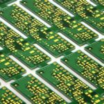
Efficient panelization and routing can help reduce manufacturing costs and improve throughput. Designers should:
- Optimize the PCB layout to maximize panel utilization and minimize waste
- Use tab routing or mouse bites for easy depanelization
- Incorporate fiducial marks and tooling holes for accurate alignment and registration
Material Selection
Careful material selection can help balance performance, reliability, and cost. Designers should:
- Choose dielectric materials with the appropriate electrical and thermal properties
- Consider the cost and availability of materials, especially for high-volume production
- Evaluate the impact of material choice on the overall system performance and reliability
Frequently Asked Questions (FAQ)
-
What is the importance of impedance matching in telecom PCB design?
Impedance matching is crucial for minimizing signal reflections and ensuring efficient power transfer. Mismatched impedances can lead to signal distortions, reduced signal integrity, and potential system failures. -
How can designers mitigate EMI in telecom PCBs?
Designers can mitigate EMI by using effective shielding techniques (e.g., grounded copper planes, shielding cans), proper grounding and power distribution, and filtering and suppression methods (e.g., LC filters, ferrite beads, TVS). -
What are some thermal management techniques for telecom PCBs?
Thermal management techniques for telecom PCBs include strategic component placement, the use of thermal vias and planes, and the incorporation of heatsinks and cooling solutions (e.g., fans, liquid cooling) for high-power applications. -
Why is design for manufacturing (DFM) important in telecom PCB design?
DFM principles help ensure that the PCB can be manufactured efficiently and with high yields. By adhering to manufacturer guidelines, using standard components, and providing adequate clearances and tolerances, designers can minimize manufacturing issues and reduce costs. -
How can designers optimize panelization and routing for cost reduction?
Designers can optimize panelization and routing by maximizing panel utilization, minimizing waste, using tab routing or mouse bites for easy depanelization, and incorporating fiducial marks and tooling holes for accurate alignment and registration.
| Aspect | Considerations |
|---|---|
| Signal Integrity | – Impedance matching – Trace routing – Via optimization |
| EMC | – Shielding – Grounding and power distribution – Filtering and suppression |
| Thermal Management | – Component placement – Thermal vias and planes – Heatsinks and cooling solutions |
| Manufacturability | – Design for manufacturing (DFM) – Panelization and routing – Material selection |
In conclusion, telecom PCB design involves a multitude of considerations to ensure reliable, high-performance, and cost-effective communication systems. By carefully addressing signal integrity, EMC, thermal management, and manufacturability aspects, designers can create telecom PCBs that meet the ever-growing demands of modern communication applications. As technology continues to advance, it is essential for designers to stay informed about the latest techniques and best practices in telecom PCB design to deliver cutting-edge solutions that drive the industry forward.
