Keyword: Circuit Board Design
Mechanical Considerations
Board Diameter and Thickness
The first step in designing a round circuit board is determining the appropriate diameter and thickness. The diameter is typically dictated by the enclosure or space constraints of the final product. Common diameters range from 10mm to 200mm, but larger or smaller sizes are possible depending on the application. The thickness of the board is usually determined by the number of layers required and the desired mechanical strength. Standard thicknesses for round PCBs include 0.8mm, 1.0mm, 1.2mm, and 1.6mm.
Mounting Holes and Cutouts
Round circuit boards often require mounting holes or cutouts to accommodate components, connectors, or mechanical features. When placing mounting holes, consider the following:
- Hole diameter: Ensure the hole size is appropriate for the mounting hardware (screws, standoffs, etc.).
- Hole placement: Position the holes symmetrically for balanced mechanical support and to avoid interfering with components or traces.
- Hole clearance: Provide adequate clearance around the holes to prevent shorting or mechanical stress.
Cutouts, such as notches or slots, may be necessary for connectors, displays, or other features. When designing cutouts, consider the following:
- Cutout shape: Choose a shape that accommodates the component or feature while maintaining board integrity.
- Cutout dimensions: Ensure the cutout size is accurate and allows for proper fitment of the component.
- Cutout position: Place cutouts strategically to minimize impact on signal integrity and mechanical strength.
Board Panelization
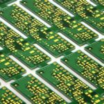
For cost-effective manufacturing, round circuit boards are often panelized, meaning multiple boards are fabricated on a single panel and then separated. When panelizing round PCBs, consider the following:
- Panel size: Choose a panel size that maximizes the number of boards per panel while allowing for adequate spacing and tooling.
- Panelization method: Options include tab routing, V-scoring, or perforating. Select a method that ensures clean separation without damaging the boards.
- Fiducial marks: Include fiducial marks on the panel for accurate registration during assembly and separation.
Electrical Considerations
Component Placement
Proper component placement is crucial for optimal electrical performance and manufacturability. When placing components on a round circuit board, consider the following:
- Component orientation: Orient components to minimize trace lengths and reduce signal interference.
- Component spacing: Provide adequate spacing between components for heat dissipation and to facilitate assembly.
- Symmetry: Place components symmetrically, when possible, to balance electrical and mechanical characteristics.
- Clearance: Ensure sufficient clearance between components and the board edge to avoid mechanical interference.
Signal Integrity
Maintaining signal integrity is essential for reliable operation of the circuit. When routing traces on a round PCB, consider the following:
- Trace width and spacing: Choose appropriate trace widths and spacing based on the signal requirements and PCB manufacturing capabilities.
- Impedance control: Use controlled impedance techniques, such as differential pairs or coplanar waveguides, for high-speed signals.
- Grounding and shielding: Implement proper grounding and shielding strategies to minimize electromagnetic interference (EMI) and crosstalk.
- Via placement: Position vias strategically to minimize signal reflections and maintain signal integrity.
Power Distribution
Efficient power distribution is crucial for stable operation and minimizing noise. When designing power distribution on a round PCB, consider the following:
- Power planes: Use dedicated power planes, when possible, to provide low-impedance power distribution.
- Decoupling capacitors: Place decoupling capacitors close to power pins of integrated circuits to suppress high-frequency noise.
- Voltage regulation: Implement voltage regulation techniques, such as linear regulators or switching regulators, to provide stable power supplies.
- Current carrying capacity: Ensure traces and planes have sufficient current carrying capacity to handle the required load.
Manufacturing Considerations
Material Selection
Selecting the appropriate material for a round circuit board depends on the electrical, mechanical, and environmental requirements of the application. Common material options include:
- FR-4: A widely used, cost-effective material with good electrical and mechanical properties.
- High-Tg FR-4: Offers improved thermal stability and reduced warpage compared to standard FR-4.
- Polyimide: Provides excellent thermal stability and flexibility for high-temperature applications.
- Metal core: Used for enhanced heat dissipation in power-intensive applications.
Copper Weight and Thickness
The copper weight and thickness of the PCB layers impact the electrical and thermal characteristics of the board. Consider the following:
- Signal layers: Typically use 1/2 oz to 1 oz copper for signal layers, depending on the current requirements.
- Power and ground planes: Use thicker copper, such as 2 oz or 4 oz, for improved current carrying capacity and thermal management.
- Plating thickness: Specify the appropriate plating thickness for through-holes and vias based on the application requirements.
Solder Mask and Silkscreen
Solder mask and silkscreen are important for protecting the board and providing identification. When designing solder mask and silkscreen for a round PCB, consider the following:
- Solder mask color: Choose a color that provides good contrast for inspection and alignment, such as green or black.
- Solder mask clearance: Provide adequate clearance around pads and vias to ensure proper solder wetting and prevent solder bridging.
- Silkscreen legibility: Use clear and concise text for component identification and orientation, ensuring legibility even on small round boards.
- Silkscreen placement: Position silkscreen markings to avoid interfering with components or assembly processes.
Testing and Validation
Design Rule Checking (DRC)
Before finalizing the design, perform thorough design rule checking to ensure the board meets manufacturing and electrical requirements. DRC checks include:
- Clearance checks: Verify that components, traces, and planes maintain the required clearances.
- Annular ring checks: Ensure vias have sufficient annular ring size for reliable connections.
- Copper spacing checks: Confirm that copper features maintain the necessary spacing for manufacturability.
- Hole size checks: Verify that drilled holes and vias meet the specified dimensions.
Prototype Testing
Once the design is finalized and prototypes are manufactured, conduct thorough testing to validate the board’s functionality and performance. Testing considerations include:
- Functional testing: Verify that the board performs its intended functions correctly.
- Signal integrity testing: Measure and analyze signal quality, including rise times, overshoot, and crosstalk.
- Power integrity testing: Validate power distribution, checking for voltage drops, ripple, and noise.
- Environmental testing: Subject the board to temperature, humidity, and vibration tests, as required by the application.
Frequently Asked Questions (FAQ)
- What are the advantages of using round circuit boards?
-
Round circuit boards offer several advantages, including:
- Improved mechanical stability and durability due to the absence of sharp corners.
- Enhanced visual aesthetics for certain applications, such as wearable devices or consumer electronics.
- Reduced manufacturing costs when panelized efficiently.
- Easier integration into circular enclosures or housings.
-
Are there any limitations to designing round circuit boards?
-
While round circuit boards offer unique benefits, they also present some limitations:
- Limited space for component placement and routing compared to rectangular boards.
- Increased complexity in panelization and assembly processes.
- Potential challenges in achieving controlled impedance for high-speed signals.
- Reduced availability of standard enclosures and mounting options.
-
How do I determine the appropriate diameter for my round circuit board?
-
The diameter of a round circuit board is primarily determined by the space constraints of the final product or enclosure. Consider the following factors:
- Required component placement and routing area.
- Mechanical clearances for mounting and assembly.
- Aesthetic considerations for the end product.
- Manufacturing capabilities and cost implications.
-
What are the common methods for panelizing round circuit boards?
-
Round circuit boards can be panelized using various methods, including:
- Tab routing: Boards are connected by small tabs that are routed out during the depaneling process.
- V-scoring: Shallow grooves are cut along the board perimeter, allowing for easy separation.
- Perforating: Small holes are drilled along the board perimeter, enabling manual separation.
- The choice of panelization method depends on the board size, material, and manufacturing requirements.
-
How can I ensure proper grounding and shielding on a round circuit board?
- Proper grounding and shielding are crucial for maintaining signal integrity and reducing EMI. Consider the following techniques:
- Use dedicated ground planes to provide a low-impedance return path for signals.
- Implement ground stitching vias to create a solid ground connection between layers.
- Apply copper pouring or guard rings around sensitive signals to minimize crosstalk.
- Incorporate shielding cans or conductive coatings for enhanced EMI protection.
- Route high-speed signals away from board edges and other sensitive areas.
Conclusion
Designing round circuit boards requires careful consideration of mechanical, electrical, and manufacturing factors. By following the guidelines and best practices outlined in this article, engineers and designers can create reliable, high-performance round PCBs that meet the unique challenges of their applications.
When designing a round circuit board, prioritize component placement, signal integrity, power distribution, and manufacturability. Use appropriate materials, copper weights, and manufacturing techniques to ensure the board functions as intended. Conduct thorough design rule checks and prototype testing to validate the design before moving to full-scale production.
By understanding the specific requirements and constraints of round circuit boards, designers can unlock new possibilities for innovative and visually appealing electronic products. With the right approach and attention to detail, round PCBs can provide a compelling solution for a wide range of applications, from wearable devices to industrial sensors and beyond.

