Semiconductors power the digital age. Integrated circuits and microchips enable advancements in computing, communications, transportation, healthcare, and virtually every industry. Fabricating these complex devices requires some of the most sophisticated and precisely controlled manufacturing processes ever developed. This article will provide an overview of the key steps used to manufacture semiconductors.
Overview of Semiconductor Fabrication
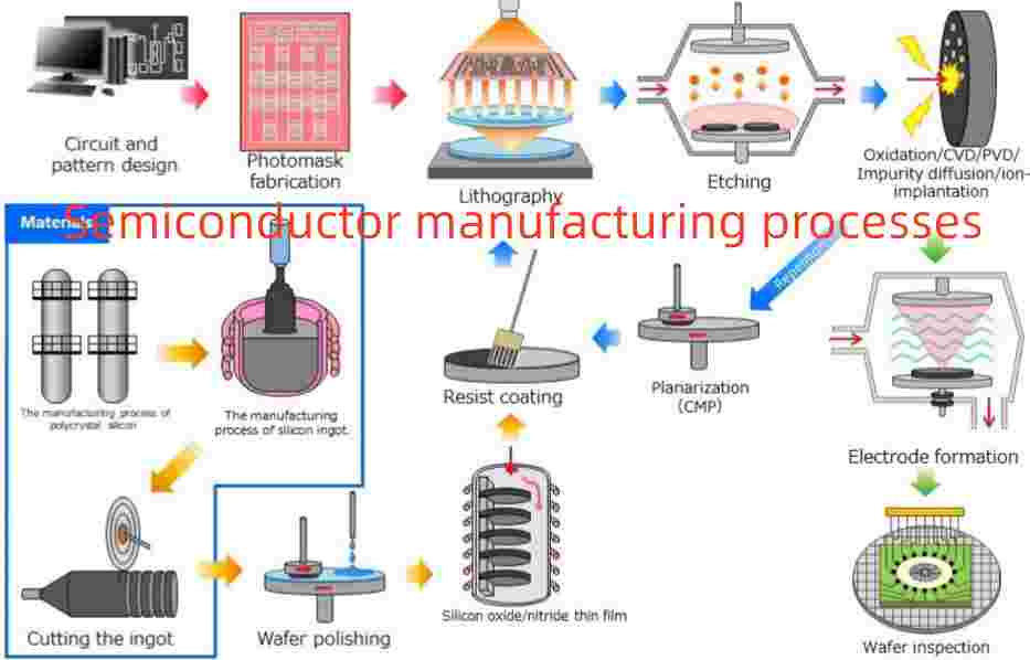
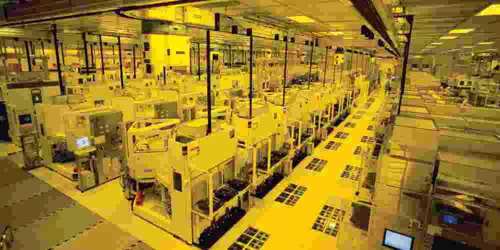
Semiconductor manufacturing transforms pure silicon crystals into integrated circuits through hundreds of highly specialized processes. Known as the fab, wafer fabrication facilities require multi-billion dollar investments and cleanroom environments. The major fabrication steps include:
1. Silicon Ingot Formation – Grow large single-crystal silicon ingots from melted high-purity polysilicon.
2. Wafer Slicing – Slice ingots into thin discs called wafers to serve as the semiconductor substrate.
3. Wafer Polishing – Grind and polish wafer surfaces to achieve extreme smoothness and uniform thickness.
4. Photomasking – Create the patterned chrome-on-glass photomasks that will define circuit geometries.
5. Wafer Cleaning/Preparation – Remove impurities and particles from wafers to ready for processing.
6. Oxidation – Grow high quality silicon oxide films which insulate the silicon wafer surface.
7. Photolithography – Transfer circuit patterns from photomasks onto photosensitive resist coatings using light exposure.
8. Etching – Remove exposed or unexposed resist areas to selectively reveal silicon wafer regions for doping or metal deposition.
9. Doping – Implant impurity atoms like boron or phosphorus into silicon to alter electrical properties in selected regions.
10. Thin Film Deposition – Deposit insulating and conductive thin film layers used to isolate and interconnect devices.
11. Chemical Mechanical Planarization (CMP) – Smoothen deposited thin films using a chemically-assisted mechanical abrasion process.
12. Wafer Testing – Electrically test devices at the wafer level to filter out defective ICs.
13. Die Preparation – Dice the wafer into individual integrated circuit chips called die.
14. Packaging – Assemble die into protective packages and wire bond pads to pins or leads.
15. Final Testing – Confirm packaged ICs function properly before shipment.
We will now examine each of these critical steps in greater detail.
Silicon Ingot Formation
Pure crystalline silicon serves as the ideal semiconducting material thanks to its elemental simplicity and abundant availability. Electronic-grade polysilicon feedstock is first purified then melted down in a precisely controlled process to grow large single silicon crystals called ingots.
Common techniques to produce monocrystalline silicon ingots are:
- Czochralski (CZ) method – Pull seed crystal from melt allowing ingot to grow as more polysilicon is added
- Float zone (FZ) method – Pass a polycrystalline rod through a molten zone to create a recrystallized ingot
- Bridgman method – Move crucible through temperature gradient allowing ingot growth from one end
Formed ingots are large cylindrical single-crystal structures up to 300mm in diameter. They exhibit an ordered atomic lattice ideal for fabricating integrated circuits.
Wafer Slicing
Ingots are sliced into discs to produce thousands of identical semiconductor wafers containing the substrate material upon which circuits will be built.
The primary technique used is ID sawing:
- Mount ingot onto rotating arbor
- Cut wafer slices from ingot using diamond-impregnated blade
- Cool and lubricate blade to minimize debris and cracking
- Achieve precisely controlled cut thickness of around 0.75mm
- Saw entire ingot into wafers sequentially
Sliced wafers exhibit mirror-smooth surface finishes. Advanced techniques like laser cutting have been introduced but ID sawing remains dominant for silicon.
Wafer Polishing
Sawed silicon wafers undergo various grinding, lapping, and polishing processes to achieve nano-smooth surfaces essential for subsequent fabrication steps. Key polishing goals:
- Remove sawing damage
- Minimize surface roughness
- Attain precisely uniform thickness
- Create flaw-free surfaces
Polishing steps include:
Grinding – Course-grind wafer backs to desired thickness using bonded abrasives
Lapping – Use progressively finer abrasive slurries on rotating plates to flatten and smooth
Mechanical polishing – Softer pad tools blend away remaining roughness and damage
Chemical mechanical planarization (CMP) – Chemically-enhanced polishing removes sub-surface damage
Repeated cycles achieve global surface flatness down to nanometer precision. Wafers must be meticulously cleaned between steps to avoid contamination.
Photomasking
Photomasks contain the circuit patterns which must be transferred to each layer of the chip. Fabricating high fidelity masks is itself a complex process:
- Chrome blank deposition – Deposit thin chrome film onto a quartz plate
- Resist coating – Spin photosensitive resist onto the chrome blank
- Pattern exposure – Use laser writer or e-beam lithography to expose the circuit pattern
- Developing – Selectively remove exposed or unexposed resist regions
- Etching – Etch away chrome not protected by resist to reveal circuit geometries
- Resist stripping and cleaning – Remove remaining resist and debris
The resulting chrome-on-glass masks define features down to 10 nanometers or less. Advanced phase shift and optical proximity correction masks further enhance patterning capabilities. Hundreds of masks are required for modern billion-transistor designs.
Wafer Cleaning and Preparation
Stringent cleaning and surface preparation are vital before commencing layer fabrication. Steps include:
- Solvent cleaning – Remove organic contaminants using acetone, alcohol, trichloroethylene
- RCA cleaning – Standard aqueous cleaning sequence to remove ionic and metal contaminants
- Surface passivation – Grow thin oxide layer to condition wafer surface
- Surface priming – Enhance photoresist adhesion using HMDS wafer coating
Many additional proprietary cleaning steps tailor wafers for specific process flows. Unwanted particles must be completely eliminated to prevent defects.
Oxidation
Silicon oxidization grows high-quality silicon dioxide films used for electrical isolation and insulation:
- Thermal Oxidation – Grow oxide layer by baking wafers in high temperature steam or oxygen rich furnaces
- Plasma Enhanced Chemical Vapor Deposition (PECVD) – Deposit oxide films from plasma-activated gas precursors
- High Density Plasma (HDP) CVD – Conformal dielectric CVD process with high deposition rates
Multiple oxidations produce gate dielectrics, diffusion masks, passivation and isolation layers. Precise control of oxidation conditions determines film quality and electrical characteristics.
Photolithography
Photolithography transfers the microscopic circuit patterns from photomasks onto the wafer layers using light exposure. This process is repeated for each layer. Key steps:
- Photoresist coating – Spin coat wafer with thin layer of photosensitive material
- Soft bake – Cure photoresist film
- Mask alignment – Precisely align mask to wafer features already formed on prior layers
- Exposure – Shine light through mask to transfer pattern into resist film
- Development – Selectively remove resist areas exposed (or unexposed) to light
- Hard bake – Further cure patterned resist prior to etching
Photolithography leverage ultraviolet and deep ultraviolet light to define ever-shrinking feature geometries. Advanced techniques like immersion lithography push patterning resolution limits.
Etching
Etching removes wafer materials in areas unprotected by photoresist, selectively revealing regions for doping or metallization. Etching types:
Wet etching – Use liquid chemicals like hydrofluoric acid to dissolve silicon
Dry etching – Reactive ion etching bombards wafer with plasma ions
Vapor phase etching – Gaseous etchants like xenon difluoride spontaneously react with exposed regions
Etching defines device geometries, contacts windows, isolation trenches and more. Tight process controls are necessary to maintain dimensional fidelity.
Doping
Doping introduces impurity atoms like boron or phosphorus into the silicon lattice in defined areas to alter electrical properties. Doping methods include:
- Ion implantation – Accelerate dopant ions into wafer and scatter them into lattice sites
- Thermal diffusion – Diffuse dopant atoms into wafer from gaseous or topical solid sources
- Plasma doping – Ionize dopants into plasma before accelerating into wafer
Doping creates p-type and n-type regions to define transistors, diodes, resistor and isolation structures. Precise doping profiles and concentrations enable device performance.
Thin Film Deposition
Depositing insulating and conducting films provides isolation between devices, conductive interconnects, and gate dielectrics. Key processes:
- Chemical vapor deposition (CVD) – React precursor gases to deposit films on wafer surfaces through chemical processes
- Physical vapor deposition (PVD) – Physically transfer material vaporized from solid targets onto the wafer by evaporation or sputtering
- Electroplating – Deposit metals by immersing wafer into electrolyte solutions with current applied
Copper, aluminum, tungsten, silicides, silicon nitride and doped glass films provide the conductive and insulating materials needed to fabricate components. Advanced deposition tools provide nanometer resolution control over film properties.
Chemical Mechanical Planarization
Chemical mechanical planarization (CMP) uses a chemically reactive liquid slurry containing abrasive particles to gently polish wafer layers flat after deposition steps. CMP:
- Produces local and global planarization
- Removes excess materials and topography
- Reduces lithography depth-of-field problems
- Prepares wafer for next process steps
The combination of chemical softening with mechanical abrasion makes CMP highly effective for achieving nano-flat wafer surfaces throughout fabrication.
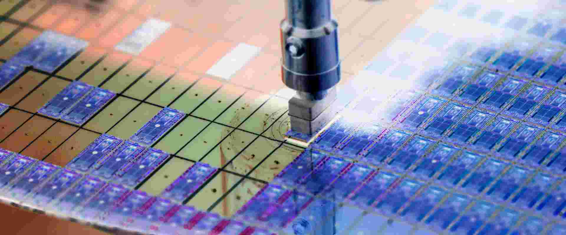
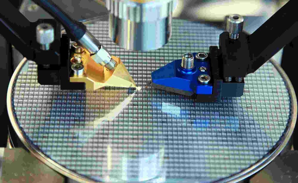
Wafer Testing
Once fabrication is complete, wafers undergo electrical testing to filter out faulty dies before assembly. Wafer probing tests:
- Parametric device metrics like threshold voltage, leakage, and gain
- Functionality of circuits, logic, and memories
- Analog characteristics like bandwidth, frequency response, distortion
- Continuity and leakage between terminals
Wafer testing eliminates dies with substandard performance due to defects or process variability. This avoids wasted packaging expense.
Die Preparation
Wafers are diced into individual integrated circuit dies either by sawing or laser cutting:
- Mount wafer onto dicing tape for mechanical support
- Precisely scribe along streets between dies with diamond saw or laser
- Use high pressure water spray to separate diced dies
Completed dies are visually inspected for flaws under microscopes. Qualified dies proceed to packaging while rejects are discarded.
Packaging
Packaging encloses and protects die, connects pads to pins, and facilitates PCB mounting. Packaging types:
- Plastic encapsulated – Molding epoxy or polymer encases wire bonded die
- Ceramic packages – Die attached and sealed into ceramic carriers
- Flip chip – Directly attach die face-down on substrate
- Wafer-level packaging – Encapsulate die while still in wafer form
Billions of semiconductor packages are manufactured annually using mass production automation. Trends favor miniaturization and density through advanced packaging.
Final Testing
Before customer delivery, packaged ICs undergo final test procedures including:
- Burn-in – Stress circuits at elevated temperature and voltage to uncover latent defects
- Parametric testing – Confirm devices function properly over full operating range
- Functional testing – Validate core logic and memories operate per specifications
- Environmental testing – Verify operation under temperature cycling, vibration, etc.
- Reliability testing – Monitor parameters over time to assess lifetime
Rigorous testing confirms devices meet design specifications and reliability targets prior to being shipped to customers.
Conclusion
These intricate steps transform common sand into the miraculous silicon chips that enable the modern digital age. Semiconductor manufacturing pushes boundaries of science and engineering to achieve nanoscale geometries with micron alignment precision through hundreds of interconnected steps. Each new generation requires unprecedented innovations to advance Moore’s Law and deliver ever more powerful chips to feed our silicon hunger.
FQA
What are some key differences between frontend and backend semiconductor manufacturing?
Frontend wafer fabrication involves steps like deposition, lithography, doping, and etching to build devices on the wafer surface. Backend assembly packages individual dies and interconnects them with the system.
Why does semiconductor fabrication require such ultraclean manufacturing environments?
Even microscopic particles can cause killer defects in densely packed chip designs with nanometer-scale features, making fanatical contamination controls essential.
What are some of the biggest challenges faced in advancing semiconductor manufacturing?
Shrinking geometries, increasing wafer sizes, complexity, variability control, defects, throughput, uptime, escalating capital costs, and resource sustainability are major ongoing challenges.
How precisely can photolithography patterning processes print integrated circuit features today?
State-of-the-art 193i immersion lithography tools with multiple patterning can resolve geometries down to around 5 nanometers for leading edge logic chips.
Why does testing play such a prominent role in semiconductor manufacturing flows?
Billions of dollars are invested in wafer fabs, making it crucial to identify and eliminate faulty dies through comprehensive testing so only fully functional devices ship.


