Introduction to Heat Sink PCBs
In the world of electronics, managing heat dissipation is a crucial aspect of designing and manufacturing reliable and efficient devices. As electronic components become more compact and powerful, the need for effective thermal management solutions has become increasingly important. One such solution is the use of Heat Sink Printed Circuit Boards (PCBs), which have gained significant attention in the electrical industry due to their ability to efficiently dissipate heat from electronic components. In this article, we will delve into the concept of Heat Sink PCBs, their construction, advantages, applications, and their importance in the electrical industry.
What is a Heat Sink PCB?
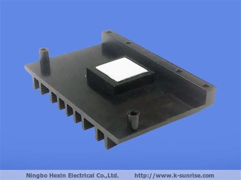
A Heat Sink PCB, also known as a thermal management PCB or a metal core PCB (MCPCB), is a specialized type of printed circuit board designed to effectively dissipate heat generated by electronic components. Unlike traditional PCBs, which primarily focus on electrical connectivity, Heat Sink PCBs incorporate a metal substrate or core that acts as a heat spreader and conducts heat away from the components.
The basic structure of a Heat Sink PCB consists of the following layers:
- Dielectric layer: This is an electrically insulating layer that separates the metal substrate from the copper circuit layer.
- Metal substrate: The metal substrate, typically made of aluminum or copper, acts as the heat spreader and provides a path for heat dissipation.
- Copper circuit layer: This layer contains the electrical traces and pads for component placement, similar to a standard PCB.
- Solder mask: The solder mask layer protects the copper traces and prevents short circuits during soldering.
- Silkscreen: The silkscreen layer provides text and symbols for component identification and assembly guidance.

Advantages of Heat Sink PCBs
Heat Sink PCBs offer several advantages over traditional PCBs when it comes to thermal management:
- Enhanced heat dissipation: The metal substrate in Heat Sink PCBs provides a highly conductive path for heat to be dissipated away from electronic components, reducing the risk of overheating and improving overall system reliability.
- Improved thermal stability: By efficiently removing heat from components, Heat Sink PCBs help maintain a stable operating temperature, which is crucial for maintaining the performance and longevity of electronic devices.
- Increased power handling capacity: With better thermal management, Heat Sink PCBs can support higher power densities and accommodate components with higher power ratings, enabling the design of more compact and efficient electronic systems.
- Reduced thermal stress: Effective heat dissipation reduces thermal stress on components, minimizing the risk of thermal-induced failures and improving the overall reliability of the electronic device.
- Compact design: Heat Sink PCBs allow for more compact designs by eliminating the need for additional heat sinks or cooling solutions, saving space and reducing overall system size.

Applications of Heat Sink PCBs
Heat Sink PCBs find applications in various industries and electronic devices where thermal management is critical. Some common applications include:
- Power electronics: Heat Sink PCBs are widely used in power electronic devices such as power converters, inverters, and motor drives, where high power densities and efficient heat dissipation are essential.
- LED lighting: LED lighting systems generate significant amounts of heat, and Heat Sink PCBs are used to dissipate heat from LED arrays, ensuring optimal performance and longevity.
- Automotive electronics: In the automotive industry, Heat Sink PCBs are used in various applications such as engine control units, power steering modules, and infotainment systems, where reliable operation in harsh environments is crucial.
- Telecommunications: Heat Sink PCBs are used in telecommunications equipment, such as base stations and routers, to manage heat generated by high-speed processors and RF components.
- Industrial automation: In industrial automation systems, Heat Sink PCBs are employed in motor drives, power supplies, and control modules to ensure reliable operation in demanding industrial environments.

Designing Heat Sink PCBs
Designing a Heat Sink PCB involves several considerations to ensure optimal thermal performance and manufacturability. Some key design aspects include:
- Material selection: Choosing the appropriate metal substrate material, such as aluminum or copper, based on thermal conductivity, weight, and cost requirements.
- Dielectric layer: Selecting a dielectric material with good thermal conductivity and electrical insulation properties, such as aluminum oxide or boron nitride.
- Thermal vias: Incorporating thermal vias, which are conductive holes drilled through the PCB, to enhance heat transfer from the components to the metal substrate.
- Component placement: Optimizing component placement to minimize thermal hotspots and ensure even heat distribution across the PCB.
- Thermal simulation: Conducting thermal simulations to analyze the heat flow and identify potential thermal issues before manufacturing the PCB.
- Manufacturing process: Considering the specific manufacturing processes and requirements for Heat Sink PCBs, such as metal substrate preparation, dielectric layer application, and circuit layer fabrication.
Manufacturing Heat Sink PCBs
The manufacturing process for Heat Sink PCBs differs from that of standard PCBs due to the presence of the metal substrate. The general manufacturing steps include:
- Metal substrate preparation: The metal substrate, typically aluminum or copper, is cleaned and treated to ensure proper adhesion of the dielectric layer.
- Dielectric layer application: The dielectric material is applied to the metal substrate, either through lamination or coating processes, to provide electrical insulation between the metal and the copper circuit layer.
- Copper foil lamination: A copper foil is laminated onto the dielectric layer to create the circuit layer.
- Circuit patterning: The desired circuit pattern is transferred onto the copper layer using photolithography and etching processes.
- Drilling and plating: Holes are drilled through the PCB for component placement and thermal vias, and the holes are plated with copper to establish electrical and thermal connections.
- Solder mask and silkscreen application: The solder mask and silkscreen layers are applied to protect the copper traces and provide component identification markings.
Thermal Management Techniques for Heat Sink PCBs
In addition to the inherent thermal management capabilities of Heat Sink PCBs, several techniques can be employed to further enhance heat dissipation and improve thermal performance:
- Thermal interface materials (TIMs): TIMs, such as thermal greases, pads, or phase change materials, can be applied between the components and the PCB to improve thermal contact and reduce thermal resistance.
- Heat spreaders: Additional heat spreaders, such as copper or aluminum plates, can be attached to the PCB to increase the heat dissipation surface area and improve overall thermal performance.
- Thermal vias: Increasing the number and density of thermal vias in the PCB can enhance heat transfer from the components to the metal substrate.
- Conformal coating: Applying a conformal coating to the PCB can provide additional protection against environmental factors and improve thermal conductivity.
- Active cooling: In some cases, active cooling solutions, such as fans or liquid cooling systems, can be used in conjunction with Heat Sink PCBs to further enhance heat dissipation.
Testing and Quality Control
To ensure the reliability and performance of Heat Sink PCBs, rigorous testing and quality control measures are implemented during the manufacturing process:
- Thermal performance testing: Thermal imaging cameras and thermocouples are used to measure the temperature distribution across the PCB and verify that the thermal design meets the specified requirements.
- Electrical testing: Electrical continuity, insulation resistance, and high-potential (hipot) tests are conducted to ensure the electrical integrity of the PCB.
- Mechanical testing: Vibration and shock tests are performed to verify the mechanical robustness of the PCB and its components.
- Environmental testing: Heat Sink PCBs are subjected to environmental tests, such as thermal cycling and humidity exposure, to assess their performance under various operating conditions.
- Visual inspection: Automated optical inspection (AOI) and manual visual inspection are used to identify any manufacturing defects or anomalies.
Future Trends in Heat Sink PCBs
As the demand for high-performance electronic devices continues to grow, the development of Heat Sink PCBs is expected to advance in several areas:
- Advanced materials: Research into new dielectric materials and metal substrates with higher thermal conductivity and better electrical insulation properties will enable the design of more efficient Heat Sink PCBs.
- Embedded components: The integration of passive components, such as resistors and capacitors, directly into the PCB substrate will reduce component count and improve thermal performance.
- 3D printing: Additive manufacturing techniques, such as 3D printing, may be used to create complex Heat Sink PCB geometries and optimize heat dissipation paths.
- Hybrid cooling solutions: The combination of Heat Sink PCBs with other cooling technologies, such as liquid cooling or thermoelectric cooling, will provide more advanced thermal management solutions for high-power applications.
- IoT and smart electronics: As the Internet of Things (IoT) and smart electronics continue to grow, Heat Sink PCBs will play a crucial role in enabling compact, reliable, and thermally efficient devices.
Conclusion
Heat Sink PCBs have emerged as a critical solution for thermal management in the electrical industry, enabling the design of compact, reliable, and high-performance electronic devices. By incorporating a metal substrate and specialized manufacturing techniques, Heat Sink PCBs efficiently dissipate heat from electronic components, improving thermal stability, power handling capacity, and overall system reliability. As electronic devices continue to evolve and become more sophisticated, the importance of Heat Sink PCBs in the electrical industry will only continue to grow, driving innovations in materials, design, and manufacturing processes.
Frequently Asked Questions (FAQ)
1. What is the difference between a Heat Sink PCB and a standard PCB?
A Heat Sink PCB incorporates a metal substrate, typically aluminum or copper, that acts as a heat spreader to dissipate heat from electronic components. In contrast, a standard PCB primarily focuses on electrical connectivity and does not have a dedicated metal layer for heat dissipation.
2. What are the advantages of using a Heat Sink PCB?
Heat Sink PCBs offer several advantages, including enhanced heat dissipation, improved thermal stability, increased power handling capacity, reduced thermal stress on components, and the ability to create more compact designs by eliminating the need for additional heat sinks.
3. What industries commonly use Heat Sink PCBs?
Heat Sink PCBs find applications in various industries, such as power electronics, LED lighting, automotive electronics, telecommunications, and industrial automation, where thermal management is critical for ensuring reliable operation and performance.
4. How does the manufacturing process of a Heat Sink PCB differ from that of a standard PCB?
The manufacturing process of a Heat Sink PCB involves additional steps compared to a standard PCB, including metal substrate preparation, dielectric layer application, and specific considerations for circuit patterning and thermal via creation.
5. What are some future trends in Heat Sink PCB technology?
Future trends in Heat Sink PCBs include the development of advanced materials with higher thermal conductivity, the integration of embedded components, the use of 3D printing for complex geometries, the combination of Heat Sink PCBs with other cooling technologies, and their increasing importance in IoT and smart electronics applications.


