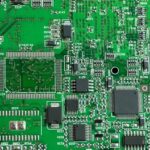
Soldering Defects in PCB Assembly
Soldering is one of the most important steps in the PCB assembly process. It’s how components are electrically and mechanically connected to the circuit board. High quality, reliable solder joints are essential for proper functionality and durability. However, the soldering process can be prone to various defects if not well controlled.
Some common soldering problems in PCB assembly include:
Bridging
Solder bridges are unintended connections between two or more solder joints or pads. They are typically caused by excess solder applied during the soldering process. Bridging can short circuit components and traces, preventing the PCB from functioning properly.
Insufficient Wetting
Also known as poor wetting, this refers to incomplete bonding between the solder and the surfaces being joined (component leads, pads). It results in a weak solder joint more prone to cracking and detachment. Insufficient flux, improper temperature profiles, and contamination can cause poor wetting.
Solder Balls
These are small spheres of solder that are inadvertently deposited on the PCB during assembly. They can cause short circuits if they lodge between pins or traces. Solder balls often result from excessive solder paste application or improper reflow oven settings.
Tombstoning
Tombstoning, also called drawbridging, is when a surface mount component stands up on one end, lifting one of its terminations off the pad. It’s usually due to an imbalance in the solder volume or wetting forces on either side of the component. Proper paste deposition and reflow profiles are key to avoiding tombstoning.
| Solder Material Selection | Effect on Defects |
|---|---|
| Lead-based | Lower melting point, better wetting, more forgiving process window; restricted due to toxicity |
| Lead-free | Higher melting point, poorer wetting, tighter process window; required in many industries for environmental reasons |
Careful control of the soldering process parameters, such as temperature ramp rates, peak temperatures, and dwell times, is critical to minimizing these types of defects, as is proper selection and application of solder materials and fluxes.
Component Placement Issues
Before soldering occurs, components must be accurately positioned and aligned on the PCB. Pickup and placement by machine or by hand can introduce a variety of defects.
Misalignment
Component misalignment is when a part is placed out of position relative to its designated location on the board. It can lead to poor solder joints or complete lack of connection if the leads/pins aren’t properly in contact with their pads. Causes include incorrect centering during pickup, shifting during transfer, or obstruction by adjacent components.
Wrong Part/Orientation
Human error or machine programming mistakes can result in the wrong component being used or a component being placed in the wrong orientation (e.g. rotated 90° or 180°). This may prevent the board from functioning as intended. Following the bill of materials and verifying the pick and place program are important safeguards.
Damaged/Defective Parts
Components themselves may have preexisting defects like bent pins, damaged packaging, or internal flaws that impact functionality. Placement force that is too high can also induce damage. Using parts from qualified vendors, inspecting for visible damage, and controlling placement parameters helps reduce these issues.
Tombstoning
As mentioned in the soldering section, tombstoning is often the result of placement issues like uneven amounts of paste on the pads or one side being heated more quickly during reflow. Precise alignment and uniform heating are key.
| Component Type | Placement Challenges |
|---|---|
| Through-hole | Requires more manual intervention, leads must be formed correctly and inserted through holes |
| Surface Mount (SMT) | Allows more automation, but smaller parts are more prone to shifting/tombstoning |
Utilizing machine vision systems to verify alignment and proper component selection, controlling placement force and speed, and maintaining the placement equipment can all help mitigate these common defects.
Design-Related Problems
Not all PCB Assembly Problems originate on the production floor. Many can be traced back to issues with the board design itself.
Manufacturability
Designs that don’t adhere to manufacturing constraints and guidelines are more prone to assembly defects. For example:
– Pads and traces that are too small or too close together
– Inadequate clearance for placement and soldering equipment
– Components that are difficult to place automatically
Involving manufacturing engineers early in the design process and following design for manufacturability (DFM) principles helps ensure designs are optimized for assembly.
Incorrect/Outdated Files
PCB assembly relies on a variety of files, including Gerber files, pick and place files, and BOMs. If these files are incorrect, outdated, or not properly transferred to manufacturing, various assembly problems can ensue. Instituting strict revision control and a robust system for handing off design files is crucial.
Footprint Mismatch
If the land pattern/footprint for a component on the PCB doesn’t match the actual physical part, it can lead to assembly issues like improper fit, skewed placement, or open solder joints. The design library must be kept up to date with accurate footprints for all specified components.
| Design Revision | Potential Impact |
|---|---|
| Initial Release | May not account for all manufacturing constraints |
| Rev 1 (DFM Optimized) | Incorporates manufacturing feedback to improve assembly yield |
| Rev 2 (ECO Change) | Engineering change orders must be clearly communicated to avoid building to the wrong revision |
Close collaboration between design and manufacturing teams, adherence to DFM guidelines, and robust processes for design transfer and revision control are all essential for avoiding design-related assembly problems.

Contamination and Residues
Cleanliness is critical in electronics manufacturing. Contamination and residues on the PCB or components can interfere with soldering, leading to defects and reliability issues.
Flux Residue
Flux is used to promote solder wetting and prevent oxidation during the soldering process. However, flux residues left behind after soldering can be corrosive or electrically conductive, leading to issues over time. No-clean fluxes minimize residue, while water soluble and rosin-based fluxes require thorough cleaning after soldering.
Handling/Finger Oils
Oils and contaminants from human handling can impede solder adhesion if boards and components aren’t kept clean during assembly. Proper use of ESD-safe gloves, minimizing handling, and regular cleaning of work surfaces helps prevent this.
Foreign Objects/Debris
Dust, fibers, hair, and other debris can cause contamination issues if they adhere to solder paste or flux. In addition to regular cleaning, using covers on PCBs and components during staging and downtime is advisable.
| Contamination Source | Potential Effect |
|---|---|
| Flux residue | Corrosion, dendrite growth, current leakage |
| Oils/Fingerprints | Poor solder wetting, adhesion issues |
| Foreign debris | Solder joint interference, short circuits |
Establishing and following robust cleaning and contamination control protocols, including verification of cleanliness at key points in the assembly process, is important for delivering high quality, reliable PCBs.
FAQ
What are some of the most common PCB assembly problems?
Some of the most frequently encountered issues in PCB assembly include soldering defects (bridging, poor wetting, solder balls, tombstoning), component placement issues (misalignment, wrong parts, damage), design-related problems (manufacturability, incorrect files, footprint mismatch), and contamination (flux residue, handling oils, foreign debris).
How can soldering defects be minimized?
Soldering defects can be reduced by carefully controlling the soldering process parameters (temperature profiles, dwell times), properly selecting and applying solder materials and fluxes, and regularly maintaining and calibrating soldering equipment. Automated optical inspection (AOI) after soldering can also catch defects for rework.
What role does PCB design play in assembly problems?
The PCB design itself can be a significant source of assembly problems if it doesn’t follow design for manufacturability (DFM) principles. Designs with overly small features, insufficient clearances, or incompatibility with assembly equipment can lead to issues. Close collaboration between design and manufacturing, adherence to DFM guidelines, and clear design transfer processes are key.
How important is cleanliness in preventing PCB assembly problems?
Maintaining a clean environment and minimizing contamination is critical in PCB assembly. Flux residues, handling oils, and foreign debris can all interfere with soldering and lead to defects or reliability issues. Establishing contamination control protocols, regularly cleaning, and verifying cleanliness during production is very important.
What can be done to avoid component placement issues?
Component placement problems can be reduced by properly programming and maintaining pick and place equipment, using machine vision systems for alignment and part verification, carefully controlling placement force and speed, and inspecting components for damage prior to placement. Accurate PCB designs and clear documentation also play a key role.
In summary, PCB assembly involves a complex interplay of materials, processes, and equipment, all of which can contribute to defects when not properly controlled. By understanding the common problems that can arise and instituting robust controls and best practices in design, material selection, process parameters, and contamination control, manufacturers can significantly improve the quality and reliability of their PCB assembly operations.
