Understanding PCB Defects
Before diving into detection strategies, it’s important to understand the types of defects that can occur in PCBs. Some common PCB defects include:
- Short circuits
- Open circuits
- Incorrect hole sizes
- Incorrect trace widths
- Copper contamination
- Solder mask defects
- Silk screen defects
- Delamination
- Warping or twisting
- Incorrect material properties
These defects can arise from various factors such as design errors, manufacturing process issues, handling damage, or environmental exposure.
Visual Inspection
Visual inspection is the most basic form of PCB Defect Detection. It involves examining the board with the naked eye or using magnifying lenses to identify any visible defects. This method is suitable for detecting surface-level defects such as:
- Scratches or cracks in the board surface
- Incorrect component placement or orientation
- Solder bridging or insufficient solder
- Contamination or foreign material on the board
While visual inspection is simple and low-cost, it has limitations. It relies on the skill and experience of the inspector and can be time-consuming for large batches of boards. Additionally, it may not detect internal or hidden defects.

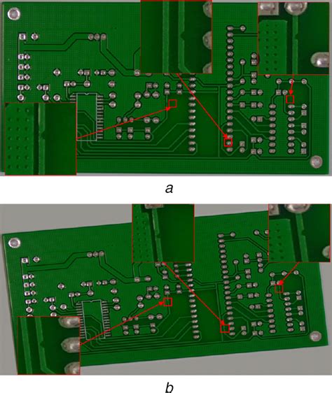
Automated Optical Inspection (AOI)
Automated Optical Inspection (AOI) is a more advanced form of visual inspection that uses cameras and image processing software to detect defects. AOI systems capture high-resolution images of the PCB from various angles and compare them to a reference image of a defect-free board. Any deviations or anomalies are flagged as potential defects.
AOI can detect a wide range of defects, including:
- Incorrect component placement or polarity
- Solder defects (bridging, insufficient, or excessive solder)
- Trace defects (open, short, or incorrect width)
- Silk screen or solder mask defects
- Contamination or foreign material
AOI offers several advantages over manual visual inspection:
- Higher speed and throughput
- Improved accuracy and consistency
- Ability to detect smaller or hidden defects
- Automated data collection and reporting
However, AOI systems can be expensive to implement and maintain. They also require proper programming and calibration to avoid false positives or false negatives.

X-Ray Inspection
X-ray inspection is a non-destructive testing method that uses X-rays to examine the internal structure of the PCB. It is particularly useful for detecting defects that are not visible on the surface, such as:
- Voids or cracks in solder joints
- Insufficient or excessive solder under components
- Broken or bent leads inside components
- Delamination or internal short circuits
X-ray inspection can be performed in two modes: 2D and 3D. 2D X-ray provides a flat image of the board, while 3D X-ray uses computed tomography (CT) to create a three-dimensional model of the board’s internal structure.
X-ray inspection offers several benefits:
- Ability to detect hidden or internal defects
- Non-destructive testing (does not damage the board)
- Can be automated for high-volume inspection
- Provides detailed images for analysis and documentation
However, X-ray inspection also has some drawbacks:
- Expensive equipment and maintenance costs
- Requires skilled operators and interpretation of images
- May not detect surface-level defects
- Potential safety hazards from X-ray exposure

Electrical Testing
Electrical testing involves applying electrical signals to the PCB and measuring its response to detect any functional or performance defects. There are several types of electrical tests:
-
Continuity Test: Checks for open or short circuits in the board’s traces and connections.
-
Insulation Resistance Test: Measures the resistance between isolated conductors to detect any leakage or insulation defects.
-
Dielectric Withstanding Voltage (DWV) Test: Applies a high voltage to the board to check for any breakdown in insulation or dielectric materials.
-
Functional Test: Verifies the board’s overall functionality by simulating its intended operation and checking for correct outputs or responses.
Electrical testing offers several advantages:
- Detects functional and performance defects that may not be visible
- Can be automated for high-volume testing
- Provides quantitative data for analysis and quality control
- Can be customized for specific board designs or applications
However, electrical testing also has some limitations:
- Requires specialized equipment and fixtures
- May not detect all types of defects (e.g., visual or mechanical defects)
- Can be time-consuming and costly for complex boards
- Potential risk of damage to the board during testing
Combining Multiple Detection Methods
No single defect detection method is perfect or comprehensive. Each method has its strengths and weaknesses, and may be better suited for certain types of defects or board designs. Therefore, many manufacturers use a combination of detection methods to ensure the highest level of quality and reliability.
For example, a typical inspection process may include:
- Visual inspection for obvious or surface-level defects
- AOI for fast and accurate detection of component and solder defects
- X-ray inspection for hidden or internal defects
- Electrical testing for functional and performance verification
By using multiple detection methods, manufacturers can catch a wider range of defects and minimize the risk of defective boards reaching the final product.
Best Practices for PCB Defect Detection
To optimize the effectiveness of PCB defect detection, manufacturers should follow some best practices:
-
Start with good design: Use design for manufacturability (DFM) principles to minimize the risk of defects in the first place.
-
Establish clear quality standards: Define acceptable levels of defects and quality criteria for each inspection method.
-
Train and qualify inspectors: Ensure that inspectors are properly trained and certified for the specific detection methods they use.
-
Calibrate and maintain equipment: Regularly calibrate and maintain inspection equipment to ensure accurate and consistent results.
-
Implement statistical process control (SPC): Use SPC techniques to monitor and control the inspection process, identify trends or anomalies, and continuously improve quality.
-
Document and analyze defects: Keep detailed records of defects found during inspection, analyze root causes, and take corrective actions to prevent recurrence.
By following these best practices, manufacturers can effectively detect and prevent PCB defects, ensuring high-quality and reliable products for their customers.
Frequently Asked Questions (FAQ)
- What is the most common type of PCB defect?
-
Solder defects, such as bridging, insufficient, or excessive solder, are among the most common types of PCB defects. These defects can cause short circuits, open circuits, or poor connections that affect the board’s functionality and reliability.
-
Can PCB defects be repaired?
-
Some PCB defects, such as minor solder defects or incorrect component placement, can be repaired using rework techniques such as soldering, desoldering, or component replacement. However, more severe defects, such as internal delamination or broken traces, may not be repairable and may require scrapping the board.
-
How much does PCB defect detection equipment cost?
-
The cost of PCB defect detection equipment varies widely depending on the type, complexity, and automation level of the equipment. Simple magnifying lenses or microscopes can cost a few hundred dollars, while advanced AOI or X-ray systems can cost hundreds of thousands or even millions of dollars. Manufacturers should carefully evaluate their quality needs and budget when selecting detection equipment.
-
What is the accuracy of PCB defect detection methods?
-
The accuracy of PCB defect detection methods depends on various factors, such as the type of defect, the inspection method, the equipment calibration, and the operator skill. In general, automated methods like AOI or X-ray inspection have higher accuracy than manual visual inspection. However, no method is 100% accurate, and manufacturers should use multiple methods and statistical process control to ensure the highest level of accuracy and quality.
-
Can PCB defect detection be outsourced?
- Yes, many manufacturers outsource PCB defect detection to specialized inspection service providers. These providers have the expertise, equipment, and capacity to handle large volumes of boards and offer a cost-effective alternative to in-house inspection. However, manufacturers should carefully evaluate the quality, reliability, and communication of the service provider before outsourcing their inspection needs.
| Defect Detection Method | Advantages | Disadvantages |
|---|---|---|
| Visual Inspection | – Low cost – Simple to implement – Detects surface-level defects |
– Time-consuming – Relies on operator skill – May miss internal or hidden defects |
| Automated Optical Inspection (AOI) | – Fast and accurate – Detects component and solder defects – Automated data collection and reporting |
– Expensive equipment and maintenance – Requires programming and calibration – May have false positives or false negatives |
| X-Ray Inspection | – Detects internal or hidden defects – Non-destructive testing – Provides detailed images for analysis |
– Expensive equipment and maintenance – Requires skilled operators – May not detect surface-level defects |
| Electrical Testing | – Detects functional and performance defects – Can be automated for high volume – Provides quantitative data for analysis |
– Requires specialized equipment and fixtures – May not detect all types of defects – Potential risk of damage to the board |
In conclusion, PCB defect detection is a critical process for ensuring the quality, reliability, and safety of electronic products. Manufacturers have a range of detection methods available, each with its own strengths and weaknesses. By understanding the types of defects, selecting the appropriate detection methods, and following best practices for inspection and quality control, manufacturers can effectively detect and prevent PCB defects, ultimately delivering high-quality products to their customers.


