Description
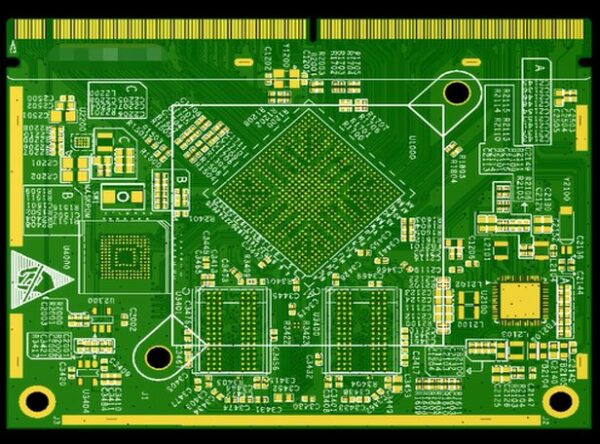
A 10-layer PCB (Printed Circuit Board) is a type of multi-layer PCB that consists of ten conductive layers separated by insulating materials. These layers are used to accommodate complex circuit designs and provide high-density interconnections between components. Here are some key points about 10-layer PCBs:
- Layer composition: A 10-layer PCB typically consists of the following layers:
- Top and bottom signal layers
- Four internal signal layers
- Four plane layers (power/ground planes)
- Increased routing density: With ten layers, PCB designers have more routing channels available, allowing for higher component density and more complex circuit designs compared to fewer layer PCBs.
- Power distribution: The dedicated power and ground planes in a 10-layer PCB provide efficient power distribution and help reduce electromagnetic interference (EMI) and crosstalk.
- Signal integrity: The controlled impedance and shorter trace lengths in multi-layer PCBs like the 10-layer design help maintain signal integrity for high-speed and high-frequency applications.
- Applications: 10-layer PCBs are commonly used in various industries, including telecommunications, networking equipment, server systems, industrial control systems, and high-end consumer electronics, where complex circuit designs and high-density packaging are required.
- Manufacturing complexity: Producing a 10-layer PCB is more complex and expensive than fewer layer PCBs due to the increased number of lamination cycles, registration requirements, and overall manufacturing complexity.
- Design considerations: Designing a 10-layer PCB requires careful planning for layer stackup, signal routing, power distribution, thermal management, and signal integrity analysis to ensure proper functionality and reliability.
- Cost and lead time: Due to the increased complexity, 10-layer PCBs generally have higher manufacturing costs and longer lead times compared to simpler PCB designs.
While 10-layer PCBs offer advantages in terms of routing density, signal integrity, and power distribution, they also require advanced design expertise, manufacturing capabilities, and higher investment compared to simpler PCB designs. The choice of a 10-layer PCB is typically driven by the complexity of the circuit design, density requirements, and performance specifications of the electronic product.